Datasheet
General description
The Infineon AIROC™ CYW20829 is a high-performance, ultra-low-power and “Secure” MCU + Bluetooth® LE platform, purpose-built for IoT applications. It combines a high-performance microcontroller with Bluetooth® LE (5.4) connectivity, high-performance analog-to-digital conversion audio input, I2S/PCM, CAN, LIN for automotive use cases and other standard communication and timing peripherals. CYW20829 employs high level of integration to minimize external components, reducing the device footprint and costs associated with implementing Bluetooth® Low Energy solutions. AIROC™ CYW20829 is the optimal solution for wireless input devices, remotes, keyboards, joysticks, Bluetooth® Mesh, automotive, asset tracking, and Bluetooth® LE IoT applications that need 10 dBm RF output power such as lighting and home automation.
Features
- 32-bit application core subsystem
- 48/96-MHz Arm® Cortex®-M33 CPU with single-cycle multiply and memory protection unit (MPU)
- Armv8-M architecture
- CMOS 40-nm process
- User-selectable core logic operation at either 1.1 V or 1.0 V
- Active CPU current slope with 1.1 V core operation
- Cortex®-M33: 40 μA/MHz
- Active CPU current slope with 1.0 V core operation
- Cortex®-M33: 22 μA/MHz
- Datawire (DMA) controller with 16 channels
- 32-KB cache for greater XIP performance with lower power
- Memory subsystem
- 256-KB SRAM with power and data retention control
- OTP eFuse array for security provisioning
- Bluetooth® Low Energy subsystem
- 48-MHz Arm® Cortex®-M33 CPU with 2.4 GHz RF transceiver with 50 Ω antenna drive
- Digital PHY
- Link layer engine supporting master and slave modes
- Programmable TX power: up to 10 dBm
- RX sensitivity:
- LE-1 Mbps: -98 dBm
- LE-2 Mbps: -95 dBm
- Coded PHY 500 kbps (LE-LR): –101 dBm
- Coded PHY 125 kbps (LE-LR): –106 dBm
- 5.2 mA TX (0 dBm), 17.2 mA TX (10 dBm), and 5.6 mA RX (LE 1 Mbps) current with 3.0 V supply and using internal buck converter
- CYW20829 link layer engine can support up to 16 connections of any combinations between central and peripheral devices simultaneously. For example, 13 central devices and three peripheral devices, or three central devices and 13 peripheral devices
- Angle of Arrival (AoA) and Angle of Departure (AoD)1
- Low-power 1.7 V to 3.6 V operation
- Six power modes for fine-grained power management
- Deep Sleep mode current of 4.5 µA with 64 KB SRAM retention
- On-chip DC-DC buck converter
- Flexible clocking options
- 8-MHz internal main oscillator (IMO) with ±2% accuracy
- Ultra-low-power 32 kHz internal low-speed oscillator (ILO)
- Two oscillators: High-frequency (24 MHz) for radio PLL and low-frequency (32 kHz watch crystal) for LPO
- 48-MHz low power IHO (internal oscillator)
- Frequency-locked loop (FLL) for multiplying IMO frequency
- Integer and fractional peripheral clock dividers
- Quad SPI
(QSPI)/serial memory interface (SMIF)
- eXecute-In-Place (XIP) from external quad SPI flash
- On-the-fly encryption and decryption
- Support for DDR
- Supports single, dual, and quad interfaces with throughput up to 384 Mbps
- Serial communication
- Three run-time configurable Serial Communication Blocks
(SCBs)
- First SCB: Configurable as SPI or I2C
- Second SCB: Configurable as SPI or UART
- Third SCB: Configurable as I2C or UART
- Only 2 instances of specific buses (SPI/I2C/UART) are possible among 3 SCBs
- Three run-time configurable Serial Communication Blocks
(SCBs)
- Audio subsystem
- Two pulse density modulation (PDM) channels and one I2S channel with time division multiplexed (TDM) mode
- Timing and pulse-width modulation
- Seven 16-bit and two 32-bit Timer/Counter Pulse-Width Modulator (TCPWM) blocks, for MCU. Multiple PWMs needed for color LEDs
- PWM supports center-aligned, edge, and pseudo-random modes
- ADC and MIC
- 12b sigma-delta switched cap ADC for audio and DC measurements
- Up to 32 programmable GPIOs
- One I/O port (8 I/Os) enables Boolean operations on GPIO pins; available during system Deep Sleep
- Programmable drive modes, strengths, and slew rates
- Two overvoltage-tolerant (OVT) pins
- Up to six, used for SMIF
- Security built into platform architecture
- ROM-based root of trust via uninterruptible “Secure Boot”
- Step-wise authentication of execution images
- Secure execution of code in execute-only mode for protected routines
- All debug and test ingress paths can be disabled
- Up to four protection contexts (One available for customer code)
- Secure debug support via authenticated debug token
- Encrypted image support for external SMIF memory
- Cryptography hardware
- Hardware Acceleration for symmetric cryptographic methods and hash functions
- True Random Number Generation (TRNG) function
- Packages
- 56-lead 6 mm x 6 mm
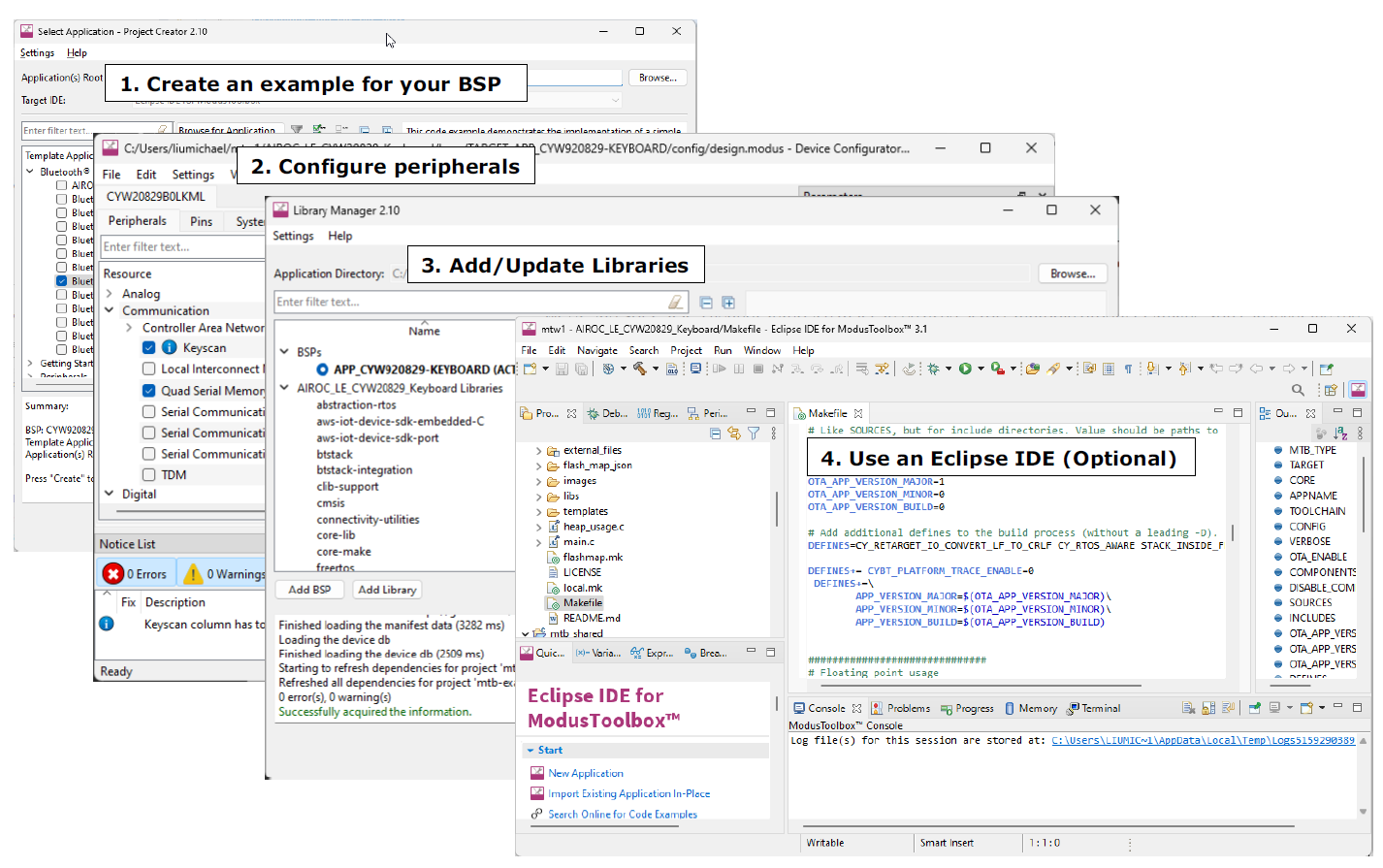
Eclipse IDE for Modustoolbox™ software
Modustoolbox™ software is Infineon’s comprehensive collection of multi-platform tools and software libraries that enable an immersive development experience for creating converged MCU and wireless systems. It is:
- Comprehensive - it has the resources you need
- Flexible - you can use the resources in your own workflow
- Atomic - you can get just the resources you want
Infineon provides a large collection of code repositories on GitHub. This includes:
- Board support packages (BSPs) aligned with Infineon kits
- Low-level resources, including a hardware abstraction layer (HAL) and peripheral driver library (PDL)
- Middleware enabling industry-leading features such as Bluetooth® Low Energy, and mesh networks
- An extensive set of thoroughly tested code example applications
ModusToolbox™ software is IDE-neutral and easily adaptable to your workflow and preferred development environment. It includes a Project Creator, a Library Manager, a BSP Assistant, peripheral and library configurators, as well as the optional Eclipse IDE for the ModusToolbox™, as Figure 1 shows. For information on using Infineon tools, refer to the documentation delivered with ModusToolbox™ software.
Block diagram
Figure 2 shows the major subsystems and a simplified view of their interconnections. The color coding shows the lowest power mode where a block is still functional. For example, the SRAM is functional down to DS-RAM mode. It should also be noted that six SMIF IOs are in addition to the 26 GPIOs listed in Figure 2.
AIROC™ CYW20829 devices include extensive support for programming, testing, debugging, and tracing both hardware and firmware. All device interfaces can be permanently disabled (device security) for applications concerned about attacks due to a maliciously reprogrammed device. All programming, debug, and test interfaces are disabled when maximum device security is enabled. The security level is settable by the user.
Complete debug-on-chip functionality enables full device debugging in the final system using the standard production device. It does not require special interfaces, debugging pods, simulators, or emulators. Only the standard programming connections are required to fully support debug.
The Eclipse IDE for ModusToolbox™ and Integrated Development Environment (IDE) provide fully integrated programming and debug support for these devices. The SWJ (SWD and JTAG) interface is fully compatible with industry-standard third party probes. With the ability to disable debug features, with very robust flash protection, and by allowing customer-proprietary functionality to be implemented in on-chip programmable blocks, CYW20829 provides a very high level of security.
Functional description
The following sections provide an overview of the features, capabilities and operation of each functional block identified in the block diagram in Figure 2. For more detailed information, refer to the following documentation:
- Board support package (BSP) documentation
BSPs are available on GitHub. They are aligned with Infineon kits and provide files for basic device functionality such as hardware configuration files, startup code, and linker files. The BSP also includes other libraries that are required to support a kit. Each BSP has its own documentation, but typically includes an API reference such as the example here. This search link finds all currently available BSPs on the Infineon GitHub site.
- Hardware abstraction layer(HAL) API reference manual
The Infineon HAL provides a high-level interface to configure and use hardware blocks on Infineon MCUs. It is a generic interface that can be used across multiple product families. You can leverage the HAL’s simpler and more generic interface for most of an application, even if one portion requires finer-grained control. The HAL API Reference provides complete details. Example applications that use the HAL download it automatically from the GitHub repository.
CPU and memory subsystem
AIROC™ CYW20829 has multiple bus masters, as Figure 2 shows. They are: CPU, datawire, QSPI, and a Crypto block. Generally, all memory and peripherals can be accessed and shared by all bus masters through multi-layer Arm® AMBA high-performance bus (AHB) arbitration. An interprocessor communication block (IPC) provides communication between the CPU and the Bluetooth® LE sub-system.
CPU
The Cortex®-M33 has single-cycle multiply and a memory protection unit (MPU). It can run at up to 96 MHz in LP mode and 48 MHz in ULP mode. This is the main CPU, designed for a short interrupt response time, high code density, and high throughput.
Cortex®-M33 implements a version of the Thumb instruction set based on Thumb-2 technology (defined in the Armv8-M architecture reference manual).
The main MCU also implements device-level security, safety, and protection features. Cortex®-M33 provides a secure, interruptible boot function. This guarantees that post boot, system integrity is checked and memory and peripheral access privileges are enforced.
The CPU has the following power draw, at VDDD = 3.0 V and using the internal buck regulator.
| System power mode | ||
|---|---|---|
| CPU | ULP | LP |
| 22 μA/MHz | 40 μA/MHz | |
The CPU can be selectively placed in Sleep and Deep Sleep power modes as defined by Arm®. The CPU also implements a Deep Sleep RAM (DS-RAM) mode in which almost all the circuits except RAM are powered OFF. Data in RAM is retained to maintain state. Upon exit, the CPU goes through a reset but can use the data in RAM to skip software initialization.
The CPU also has nested vectored interrupt controllers (NVIC) for rapid and deterministic interrupt response, and wake up interrupt controllers (WIC) for CPU wake up from Deep Sleep power mode.
CYW20829 has a debug access port (DAP) that acts as the interface for device programming and debug. An external programmer or debugger (the “host”) communicates with the DAP through the device serial wire debug (SWD) or Joint Test Action Group (JTAG) interface pins. Through the DAP (and subject to device security restrictions), the host can access the device memory and peripherals as well as the registers in the CPU.
CPU debug and trace features are as follows:
- Six hardware breakpoints and four watchpoints, serial wire viewer (SWV), and printf()-style debugging through the single wire output (SWO) pin
Interrupts
The CPU has interrupt request lines (IRQ), with the interrupt source ‘n’ directly connected to IRQn.
Each interrupt supports eight configurable priority levels. One system interrupt can be mapped to the CPU non-maskable interrupts (NMI). Multiple interrupt sources are capable of waking the device from Deep Sleep power mode using the WIC.
Datawire
Datawire is a light weight DMA controller with 16 channels, which support CPU-independent accesses to memory and peripherals. The descriptors for the channels are in SRAM and the number of descriptors is limited only by the size of the memory. Each descriptor can transfer data in two nested loops with configurable address increments to the source and destination.
Cryptography accelerator (Cryptolite)
A combination of HW and SW is able to support several cryptographic functions. Specifically it supports the following functions:
- Encryption/decryption
- AES-128 hardware accelerator with following supported modes:
- Electronic Code Book (ECB)
- Cipher Block Chaining (CBC)
- Cipher Feedback (CFB)
- Output Feedback (OFB)
- Counter (CTR)
- AES-128 hardware accelerator with following supported modes:
- Hashing
- Secure Hash Algorithm (SHA-256) hardware accelerator
- Message Authentication Functions (MAC)
- Hashed Message Authentication Code (HMAC) acceleration using SHA-256 hardware
- True Random Number Generator (TRNG)
- Vector unit hardware accelerator
- Digital Signature Verification using RSA
- Digital Signature Verification using ECDSA
Protection units
CYW20829 has multiple types of protection to control erroneous or unauthorized access to memory and peripheral registers.
Protection units support memory and peripheral access attributes including address range, read/write, code/data, privilege level, secure/non-secure, and protection context.
Protection units are configured at “Secure Boot” to control access privileges and rights for bus masters and peripherals. Up to eight protection contexts (“Secure Boot” is in protection context 0) allow access privileges for memory and system resources to be set by the “Secure Boot” process per protection context by bus master and code privilege level. Multiple protection contexts are available.
AES-128
AES-128 component to accelerate block cipher functionality. This functionality supports forward encryption of a single 128 bit block with a 128 bit key. SHA-256 component to accelerate hash functionality. This component supports message schedule calculation for a 512-bit message chunk and processing of a 512-bit message chunk.
Vector unit (VU)
VU component to accelerate asymmetric key cryptography (for example, RSA and ECC). This component supports large integer multiplication, addition, and so on. TRNG component based on a set of ring oscillators.
The TRNG includes a HW health monitor.
Controller area network flexible data-rate (CAN FD)
CYW20829 supports the CAN FD controller that supports one CAN FD channel. All CAN FD controllers are compliant with the ISO 11898-1:2015 standard; an ISO 16845:2015 certificate is available. It also implements the time-triggered CAN (TTCAN) protocol specified in ISO 11898-4 (TTCAN protocol levels 1 and 2) completely in hardware. All functions concerning the handling of messages are implemented by the RX and TX handlers. The RX handler manages message acceptance filtering, transfer of received messages from the CAN core to a message RAM, and provides receive-message status. The TX handler is responsible for the transfer of transmit messages from the message RAM to the CAN core, and provides transmit-message status. CAN FD is only available in CYW20829B0010.
Local interconnect network (LIN)
CYW20829 contains a LIN channel. Each channel supports transmission/reception of data following the LIN protocol according to ISO standard 17987. Each LIN channel connects to an external transceiver through a 3-pin interface (including an enable function) and supports master and slave functionality. Each block also supports classic and enhanced checksum, along with break detection during message reception and wake-up signaling. Break detection, sync field, checksum calculations, and error interrupts are handled in hardware. LIN is only available in CYW20829B0010.
Real time clock (RTC)
- Year/Month/Date, Day-of-week, Hour: Minute: Second fields
- 12 and 24 hour formats
- Automatic leap-year correction
Memory
CYW20829 contains the SRAM, ROM, and eFuse memory blocks.
- SRAM: CYW20829 has 256-KB of SRAM. Power control and retention granularity is 64-KB blocks allowing the user to control the amount of memory retained in Deep Sleep. Memory is not retained in Hibernate mode.
- ROM: The 64-KB ROM, also referred to as the supervisory ROM (SROM), provides code (ROM Boot) for several system functions. The ROM contains, primarily device initialization and security. ROM code is executed, in protection context 0.
- eFuse: A one-time programmable (OTP) eFuse array consists of 1024 bits, which are reserved for system use such as Die ID, Device ID, initial trim settings, device life cycle, and security settings. Some of the bits are available for storing security key information and hash values and can be programmed by the user for device security. Each fuse is individually programmed; once programmed (or “blown”), its state cannot be changed. Blowing a fuse transitions it from the default state of ‘0’ to ‘1’. To program an eFuse, VDDIO1 must be at 2.5 V ±5%. Because blowing an eFuse is an irreversible process, programming is recommended only in mass production under controlled factory conditions by Infineon provided provisioning tools.
Boot code
On a device reset, the boot code in ROM is the first code to execute. This code performs the following:
- Device trim setting (calibration)
- Setting the device protection units
- Setting device access restrictions for secure life cycle states
- Configures the Debug Access Port
- In secure life cycle supports secure debug via authenticated debug token
- Configures the SMIF for external flash access
- In secure life cycle validates first user code in external flash by checking its digital signature. Supports OTF decryption of encrypted images in external flash
- Copies the application bootstrap from the external flash to SRAM and jumps to the ROM. It cannot be changed and acts as the Root of Trust in a secure system
It should also be noted that the ROM code sets the system clock to 48 MHz IHO source.
Memory map
The 32-bit (4 GB) address space is divided into the regions shown in Table 3. Note that code can be executed from the Code, and Internal RAM or External flash.
| Address range | Name | Use |
|---|---|---|
| 0x0000 0000 – 0x1FFF FFFF | Code | Program code region. It includes the exception vector table, which starts at address 0 |
| 0x2000 0000 – 0x3FFF FFFF | SRAM | Data region |
| 0x4000 0000 – 0x5FFF FFFF | Peripheral | All peripheral registers. Code cannot be executed from this region. Bit-band in this region is not supported |
| 0x6000 0000 – 0x8FFF FFFF | External NVM | SMIF/Quad SPI (see the QSPI interface serial memory interface (SMIF). Code can be executed from this region |
| 0xA000 0000 – 0xDFFF FFFF | External Device | Not used |
| 0xE000 0000 – 0xE00F FFFF | Private Peripheral Bus | Provides access to peripheral registers within the CPU core |
| 0xE010 0000 – 0xFFFF FFFF | Device | Device-specific system registers |
The device memory map is shown in Table 3.
| Address range | Memory type | Size |
|---|---|---|
| 0x0000 0000 – 0x0001 0000 | ROM | 64 KB |
| 0x2000 0000 - 0x 2004 0000 | SRAM | Up to 256 KB |
System resources
Power system
The power system provides assurance that voltage levels are as required for each respective mode and will either delay mode entry (on power-on reset (POR), for example) until voltage levels are as required for proper function or generate resets (brownout detect (BOD)) when the power supply drops below specified levels. The design guarantees safe chip operation between power supply voltage dropping below specified levels (for example, below 1.7 V) and the reset occurring. There are no voltage sequencing requirements. CYW20829 does not support POR/BOD to guarantee EFUSE programming voltage.
The VDDD supply (1.7 V to 3.6 V) powers an on-chip buck regulator which offers a selectable (1.0 V or 1.1 V) core operating voltage (VCCD). The selection lets users choose between two system power modes:
- System Low Power (LP) operates VCCD at 1.1 V and offers high performance, with no restrictions on device configuration
- System Ultra Low Power (ULP) operates VCCD at 1.0 V for exceptional low power, but imposes limitations on clock speeds
The Bluetooth® radio requires 1.1 V for operation. Bluetooth® system may override user core voltage selection when the radio is turned on. System voltage will return to the user selected value automatically once Bluetooth® radio activity is completed. Refer to Power supply considerations for more details.
Power modes
CYW20829 can operate in four system and three CPU power modes. These modes are intended to minimize the average power consumption in an application. For more details on power modes and other power-saving configuration options, see the relevant application note.
Power modes supported by CYW20829, in the order of decreasing power consumption, are:
- System Low-power (LP) - All peripherals and CPU power modes are available at maximum speed
- System Ultra Low-power (ULP) - All peripherals and CPU power modes are available, but with limited speed
- CPU Active - CPU is executing code in system LP or ULP mode
- CPU Sleep - CPU code execution is halted in system LP or ULP mode
- CPU Deep Sleep - CPU code execution is halted and system Deep Sleep is requested in system LP or ULP mode
- System Deep Sleep - only low-frequency peripherals are available after both CPUs enter CPU Deep Sleep mode
- System Hibernate - Device and I/O states are frozen and the device resets on wakeup. Multiple sources available to wake up from this mode, including RTC, P0.5 and P1.4
- Deep Sleep RAM - only RAM and IO states are retained. All system activity except for select low power peripherals ceases until system exits from this state. The CPU resets upon exit but can skip software initialization since RAM is retained
CPU Active, Sleep, and Deep Sleep are standard Arm®-defined power modes supported by the Arm® CPU instruction set architecture (ISA). System LP, ULP, Deep Sleep, Deep Sleep RAM and Hibernate modes are additional low-power modes supported by the CYW20829.
CYW20829 clock system
CYW20829 clock system consists of a combination of oscillators, external clock, and frequency-locked loop.
Specifically, the following:
- Internal main oscillator (IMO)
- Internal low-speed oscillator (ILO)
- Watch crystal oscillator (WCO)
- System 24 MHz crystal oscillator
- External clock input
- One frequency-locked loop (FLL)
- Internal high-speed oscillator (IHO)
Clocks may be buffered and brought out to a pin on a smart I/O port.
Table 4 shows the mapping of port and associated clock group mapped to peripherals.
| PCLK group | Root clock (clk_hf) | Peripherals | Frequency | Description | |
|---|---|---|---|---|---|
| LP (1.1 V Typ) | ULP (1.0 V Typ) | ||||
| 0 | clk_hf0 | CPU Trace | 24 MHz | 24 MHz | - |
| 1 | clk_hf1 | SCB | 96 MHz | 48 MHz | Async peripherals: Strobe signals are driven through dividers; Interface clock is generated inside the peripheral with the main group clock |
| TCPWM | |||||
| LIN | |||||
| CANFD | |||||
| SMARTIO | |||||
| 2 | clk_hf0 | SMIF | 96 MHz | 48 MHz | Direct connection pass through from clk_hf. This clock is not used for interface clock, rather it is used for the MMIO clocks of SMIF, BTSS and CRYPTO. BTSS uses this clock for Master and Slave AHB/MMIO transactions, and SMIF also uses this clock for FAST/SLOW clocks |
| BTSS | |||||
| CRYPTO | |||||
| 3 | clk_hf1 | PDM | 96 MHz | 48 MHz | Uses PERI ACLK with default div by 2 option, required interface frequencies are obtained by further division inside the peripheral |
| TDM | |||||
| 4 | clk_hf2 | BTSS | 48 MHz | 48 MHz | RPU clock for BTSS |
| 5 | clk_hf3 | ADCMIC | 24 MHz | 24 MHz | Direct connection for ADCMIC, main source of clk_hf3 is clk_althf which is the BTSS ECO clock |
| 6 | clk_hf1 | SMIF | 96 MHz | 48 MHz | Direct connection for SMIF and SMARTIO peripherals. This clock is an interface clocks for these peripherals |
Internal main oscillator (IMO)
The IMO is the primary source of internal clocking. It is trimmed during testing to achieve the specified accuracy.
The IMO default frequency is 8 MHz and tolerance is ±2%.
Internal low-speed oscillator (ILO)
The ILO is a very low power oscillator, nominally 32 kHz, which operates in all power modes.
Precision internal low-speed oscillator (PILO)
The PILO is a precision low-power oscillator running at 32 kHz. It is factory calibrated to meet Bluetooth® Low Energy requirements. Like the ILO, it can operate in all power modes.
Main crystal oscillator
CYW20829 uses a 24 MHz crystal oscillator (XTAL).
The XTAL must have an accuracy as defined by the Bluetooth® specification. Two external load capacitors are required to work with the crystal oscillator. The selection of the load capacitors is XTAL-dependent (see Figure 4).
| Parameter | Symbol | Electrical specification | Note | |||
|---|---|---|---|---|---|---|
| Min | Typ | Max | Unit | |||
| Nominal frequency | FL | 24.00 | MHz | – | ||
| Oscillation mode | – | Fundamental | – | – | ||
| Load capacitance | CL | 8 | pF | – | ||
| Frequency tolerance | – | ±10 | ppm | at 25°C ± 3°C | ||
| Frequency stability | – | ± 20 | ppm | Over operating temperature range (reference 25°C) | ||
| Operating temperature | – | –40 | – | 105 | °C | – |
| Aging | – | ±3 | ppm | 1st year at 25°C ± 3°C | ||
| Drive level | DL | – | 100 | 200 | uW | – |
| Series resonant resistance | Rr | – | – | 60 | Ω | – |
| Shunt capacitance | C0 | – | – | 3 | pF | – |
| Insulation resistance | – | 500 | – | – | MΩ | at DC 100 V |
| Storage temperature range | – | –40 | – | 125 | °C | – |
32 kHz crystal oscillator
CYW20829 includes a 32 kHz oscillator to provide accurate timing during low power operations. Figure 5 shows the 32 kHz XTAL oscillator with external components and Table 6 lists the oscillator’s characteristics. This oscillator can be operated with a 32 kHz or 32.768 kHz crystal oscillator or be driven with a clock input at similar frequency. The XTAL must have an accuracy of ±250 ppm or better per the Bluetooth® spec over temperature and including aging. The default component values are: C1 = C2 = ~6 pF. The values of C1 and C2 are used to fine-tune the oscillator.
| Parameter | Sym | Conditions | Min | Typ | Max | Unit |
|---|---|---|---|---|---|---|
| Output frequency | Foscout | – | – | 32.768 | – | kHz |
| Frequency tolerance | – | Over temperature and aging | – | – | 250 | ppm |
| XATL driver level | Pdrv | For crystal selection | – | 0.1 | 0.5 | µW |
| XTAL series resistance | Rseries | For crystal selection | – | – | 70 | KΩ |
| XATL shunt capacitance | Cshunt | For crystal selection | – | – | 2.2 | pF |
Watchdog timers (WDT, MCWDT)
CYW20829 has one WDT and two multi-counter WDTs (MCWDTs). The WDT has a 16-bit free-running counter. Each MCWDT has two 16-bit counters and one 32-bit counter, with multiple operating modes. All of the 16-bit counters can generate a watchdog device reset. All of the counters can generate an interrupt on a match event.
The WDT is clocked by the ILO. It can do interrupt/wakeup generation in system LP/ULP, Deep Sleep, and Hibernate power modes. The MCWDTs are clocked by LFCLK (ILO or WCO). It can do periodic interrupt/wakeup generation in system LP/ULP and Deep Sleep power modes.
Clock dividers
Integer and fractional clock dividers are provided for peripheral use and timing purposes. There are one or more:
- 8-bit clock dividers
- 16-bit integer clock dividers
- 16.5-bit fractional clock dividers
- 24.5-bit fractional clock divider
Trigger routing
CYW20829 contains a trigger multiplexer block. This is a collection of digital multiplexers and switches that are used for routing trigger signals between peripheral blocks and between GPIOs and peripheral blocks.
There are two types of trigger routing. Trigger multiplexers have reconfigurability in the source and destination. There are also hardwired switches called “one-to-one triggers”, which connect a specific source to a destination. The user can enable or disable the route.
Reset
CYW20829 can be reset from a variety of sources:
- Power-on reset (POR) to hold the device in reset while the power supply ramps up to the level required for the device to function properly. POR activates automatically at power-up
- Brown-out detect (BOD) reset to monitor the digital voltage supply VDDD and generate a reset if VDDD falls below the minimum required logic operating voltage
- External reset dedicated pin (XRES) to reset the device using an external source. The XRES pin is active LOW. It can be connected either to a pull-up resistor to VDDD, or to an active drive circuit, as Figure 6 shows. If a pull-up resistor is used, select its value to minimize current draw when the pin is pulled LOW; 10 kΩ is typical
- Watchdog Timer (WDT or MCWDT) to reset the device if firmware fails to service it within a specified timeout period
- Software-initiated reset to reset the device on demand using firmware
- Logic-protection fault can trigger an interrupt or reset the device if unauthorized operating conditions occur; for example, reaching a debug breakpoint while executing privileged code
- Hibernate wakeup reset to bring the device out of the system Hibernate low-power mode
Reset events are asynchronous and guarantee reversion to a known state. Some of the reset sources are recorded in a register, which is retained through reset and allows software to determine the cause of the reset.
Bluetooth® LE radio and subsystem
The physical layer consists of the digital PHY and the RF transceiver that transmits and receives Gaussian frequency shift keying (GFSK) packets at 1 or 2 Mbps over a 2.4 GHz ISM band, The device also supports Bluetooth® LE long range, both 500 and 125 kbps speeds.
The baseband controller is a composite hardware and firmware implementation that supports both master and slave modes. Key protocol elements, such as HCI and link control, are implemented in firmware. Time-critical functional blocks, such as encryption, CRC, data whitening, and access code correlation, are implemented in hardware (in the LL engine).
The RF transceiver contains an integrated balun, which provides a single-ended RF port pin to drive a 50 Ω antenna via a matching/filtering network. In the receive direction, this block converts the RF signal from the antenna to a digital bit stream after performing GFSK demodulation. In the transmit direction, this block performs GFSK modulation and then converts a digital baseband signal to a radio frequency before transmitting it through the antenna.
Programmable analog-to-digital converter (ADC)
Sigma delta ADC
The ADC block is a single switched-cap Σ-Δ ADC core for audio and DC measurement. It operates at the 12-MHz clock rate and has eight GPIO inputs. The internal bandgap reference has ±5% accuracy without calibration. Different calibration and digital correction schemes can be applied to reduce ADC absolute error and improve measurement accuracy in DC.
One of three internal references may be used for the ADC reference voltage: VDDA, VDDA/2, and an analog reference (AREF). AREF is nominally 1.2 V, trimmed to ±1%.
Programmable digital
- System Deep Sleep operation
- Asynchronous or synchronous (clocked) operation
- Can be synchronous or asynchronous
Fixed-function digital
Timer/counter/pulse-width modulator (TCPWM) block
- The TCPWM supports the following operational modes:
- Timer-counter with compare
- Timer-counter with capture
- Quadrature decoding
- Pulse width modulation (PWM)
- Pseudo-random PWM
- PWM with dead time
- Up, down, and up/down counting modes
- Clock pre-scaling (division by 1, 2, 4,....64, 128)
- Double buffering of compare/capture and period values• Underflow, overflow, and capture/compare output signals
- Supports interrupt on:
- Terminal count - Depends on the mode; typically occurs on overflow or underflow
- Capture/compare - The count is captured to the capture register or the counter value equals the value in the compare register
- Complementary output for PWMs
- Selectable start, reload, stop, count, and capture event signals for each TCPWM; with rising edge, falling edge, both edges, and level trigger options. The TCPWM has a Kill input to force outputs to a predetermined state.
In this device there are:
- Two 32-bit TCPWMs
- Seven 16-bit TCPWMs
Serial communication blocks (SCB)
- This product line has three SCBs:
- First SCB: Configurable as SPI or I2C
- Second SCB: Configurable as SPI or UART
- Third SCB: Configurable as I2C or UART
- One SCB (SCB #0) can operate in system Deep Sleep mode with an external clock; this SCB can be either SPI slave or I2C slave
- I2C mode: The SCB can implement a full multi-master and slave interface (it is capable of multimaster arbitration). This block can operate at speeds of up to 1 Mbps (Fast Mode Plus). It also supports EZI2C, which creates a mailbox address range and effectively reduces I2C communication to reading from and writing to an array in the memory. The SCB supports a 256-byte FIFO for receive and transmit. The I2C peripheral is compatible with I2C standard-mode, Fast Mode, and Fast Mode Plus devices. The I2C bus I/O is implemented with GPIO in open-drain modes.
- UART mode: This is a full-feature UART operating at up to 8 Mbps. It supports automotive single-wire interface (LIN) (only available for CYW20829B0010), infrared interface (IrDA), and SmartCard (ISO 7816) protocols, all of which are minor variants of the basic UART protocol. In addition, it supports the 9-bit multiprocessor mode that allows the addressing of peripherals connected over common Rx and Tx lines. Common UART functions such as parity error, break detect, and frame error are supported. A 256-byte FIFO allows much greater CPU service latencies to be tolerated
- SPI mode: The SPI mode supports full SPI, Secure Simple Pairing (SSP) (essentially adds a start pulse that is used to synchronize SPI Codecs), and Microwire (half-duplex form of SPI). The SPI block supports an EZSPI mode in which the data interchange is reduced to reading and writing an array in memory. The SPI interface operates with a 24-MHz clock
QSPI interface serial memory interface (SMIF)
A serial memory interface is provided, running at up to 48 MHz. It supports single, dual and quad SPI configurations, and supports up to four external memory devices. It supports two modes of operation:
- Memory-mapped I/O (MMIO), a command mode interface that provides data access via the SMIF registers and FIFOs
- Execute-in-Place (XIP), in which AHB reads and writes are directly translated to SPI read and write transfers
In XIP mode, the external memory is mapped into the CYW20829 internal address space, enabling code execution directly from the external memory. To improve performance, a 32 KB cache is included. XIP mode also supports AES-128 based on-the-fly encryption and decryption, enabling secure storage and access of code and data in the external memory.
GPIO
CYW20829 has up to 32 GPIOs, which implement:
- • Eight drive strength modes:
- Analog input mode (input and output buffers disabled) on some IOs
- Input only
- Weak pull-up with strong pull-down
- Strong pull-up with weak pull-down
- Open drain with strong pull-down
- Open drain with strong pull-up
- Strong pull-up with strong pull-down
- Weak pull-up with weak pull-down
- Hold mode for latching previous state (used for retaining the I/O state in system Hibernate and deep sleep mode)
- Selectable slew rates for dV/dt-related noise control to improve EMI
The pins are organized in logical entities called ports, which are up to eight pins in width. Data output and pin state registers store, respectively, the values to be driven on the pins and the input states of the pins.
Every pin can generate an interrupt if enabled; each port has an interrupt request (IRQ) associated with it.
The port 4 pins are capable of overvoltage-tolerant (OVT) operation, where the input voltage may be higher than VDDD. OVT pins are commonly used with I²C, to allow powering the chip OFF while maintaining a physical connection to an operating I²C bus without affecting its functionality.
GPIO pins can be ganged to source or sink higher values of current. GPIO pins, including OVT pins, may not be pulled up higher than the absolute maximum; see Electrical specifications.
During power-on and reset, the pins are forced to the analog input drive mode, with input and output buffers disabled, so as not to crowbar any inputs and/or cause excess turn-on current.
A multiplexing network known as the high-speed I/O matrix (HSIOM) is used to multiplex between various peripheral and analog signals that may connect to an I/O pin.
In order to get the best performance, the following frequency and drive mode constraints may be applied. The values (refer to Table 7) represent drive strengths.
| Ports | Maximum frequency | Drive strength for VDDD < 2.7 V | Drive strength for VDDD > 2.7 V |
|---|---|---|---|
| Ports 0, 1 | 8 MHz | Up to 4 mA | Up to 8 mA |
| Ports 2 to 5 | 16 MHz; 24 MHz for SPI | Up to 4 mA | Up to 8 mA |
Special-function peripherals
Audio subsystem
The audio subsystem is only available in CYW20829B0010, it consists of the following hardware blocks:
- One inter-IC sound (I2S) interface
- Two pulse-density modulation (PDM) to pulse-code modulation (PCM) decoder channels
The I2S interface implements two independent hardware FIFO buffers - TX and RX, which can operate in master or slave mode. The following features are supported:
- Multiple data formats - I2S, left-justified, Time Division Multiplexed (TDM) mode A, and TDM mode B
- Programmable channel/word lengths - 8/16/18/20/24/32 bits
- Internal/external clock operation. Up to 192 ksps
- Interrupt mask events - trigger, not empty, full, overflow, underflow, watchdog
- Configurable FIFO trigger level with datawire support
The I2S interface is commonly used to connect with audio codecs, simple DACs, and digital microphones. The PDM-to-PCM decoder implements a single hardware Rx FIFO that decodes a stereo or mono 1-bit PDM input stream to PCM data output. The following features are supported:
- Programmable data output word length - 16/18/20/24 bits
- Configurable PDM clock generation. Range from 384 kHz to 3.072 MHz
- Droop correction and configurable decimation rate for sampling; up to 48 ksps
- Programmable high-pass filter gain
- Interrupt mask events - not empty, overflow, trigger, underflow
- Configurable FIFO trigger level with DMA support
The PDM-to-PCM decoder is commonly used to connect to digital PDM microphones. Up to two microphones can be connected to the same PDM data line.
Pinouts
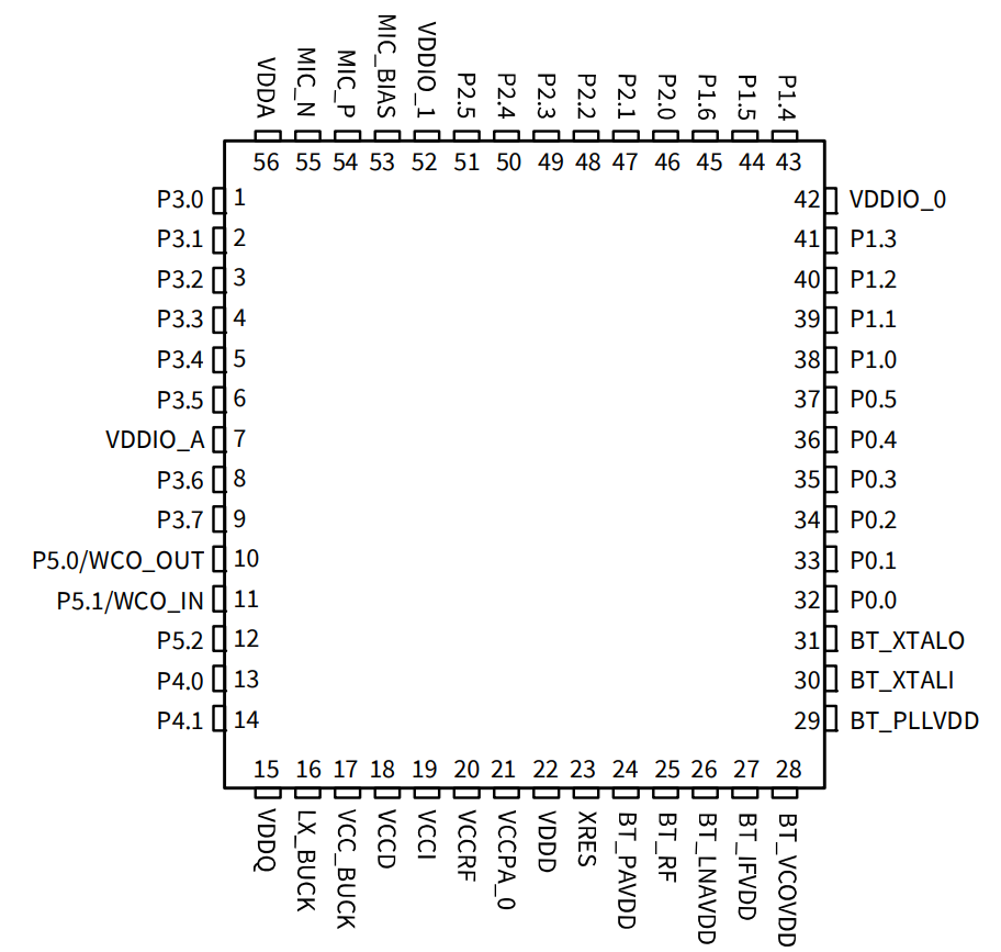
| Pin name | Pin number | I/O | Power domain | Description |
|---|---|---|---|---|
| 56-lead | ||||
| Microphone | ||||
| MIC_P | 54 | I | VDDA | Microphone positive input |
| MIC_N | 55 | I | VDDA | Microphone negative input |
| MIC_BIAS | 53 | O | VDDA | Microphone bias supply |
| Onboard switching regulator and LDOs | ||||
| VDDQ | 15 | I | - | External supply to PMU analog |
| VCC_BUCK | 17 | I | - | External supply to switching regulator |
| LX_BUCK | 16 | O | - | Switching regulator output |
| VCCD | 18 | O | - | Digital LDO output |
| VCCI | 19 | I | - | RF and digital LDO input |
| Baseband supply | ||||
| VDDIO_0 | 42 | I | VDDIO_0 | Supply for GPIO ports |
| VDDIO_1 | 52 | I | VDDIO_1 |
Supply for GPIO ports and eFuse programming. See Table 11 for eFuse programming requirements. |
| VDDIO_A | 7 | I | VDDIO_A | Supply for analog GPIO ports |
| VDDA | 56 | I | VDDA | Analog power supply voltage |
| RF power supply | ||||
| VCCRF | 20 | O | - | RFLDO output |
| VDDD | 22 | I | - | PALDO and sub-system resources supply |
| VCCPA_0 | 21 | O | - | PALDO output |
| BT_VCOVDD | 28 | I | BT_VCOVDD | VCO supply |
| BT_LNAVDD | 26 | I | BT_LNAVDD | LNA supply |
| BT_IFVDD | 27 | I | BT_IFVDD | IFPLL power supply |
| BT_PLLVDD | 29 | I | BT_PLLVDD | RFPLL and crystal oscillator supply |
| BT_PAVDD | 24 | I | BT_PAVDD | Internal PA supply |
| Radio I/O | ||||
| BT_RF | 25 | I/O | BT_RF | RF antenna port |
| Crystal | ||||
| BT_XTALI | 30 | I | BT_PLLVDD | Crystal oscillator input. Two external load capacitors are required to work with the crystal oscillator. The selection of the load capacitors is XTAL-dependent. |
| BT_XTALO | 31 | O | BT_PLLVDD | Crystal oscillator output |
| GPIO | ||||
| P0.0 | 32 | I/O | VDDIO_0 | General input and output port. See
Table 9 for alternate functions. P0.5 and P1.4 can be used as the wake source for hibernate mode |
| P0.1 | 33 | I/O | VDDIO_0 | |
| P0.2 | 34 | I/O | VDDIO_0 | |
| P0.3 | 35 | I/O | VDDIO_0 | |
| P0.4 | 36 | I/O | VDDIO_0 | |
| P0.5 | 37 | I/O | VDDIO_0 | |
| P1.0 | 38 | I/O | VDDIO_0 | |
| P1.1 | 39 | I/O | VDDIO_0 | |
| P1.2 | 40 | I/O | VDDIO_0 | |
| P1.3 | 41 | I/O | VDDIO_0 | |
| P1.4 | 43 | I/O | VDDIO_0 | |
| P1.5 | 44 | I/O | VDDIO_0 | |
| P1.6 | 45 | I/O | VDDIO_0 | |
| P2.0 | 46 | I/O | VDDIO_0 | |
| P2.1 | 47 | I/O | VDDIO_0 | |
| P2.2 | 48 | I/O | VDDIO_0 | |
| P2.3 | 49 | I/O | VDDIO_0 | |
| P2.4 | 50 | I/O | VDDIO_0 | |
| P2.5 | 51 | I/O | VDDIO_0 | |
| P3.0 | 1 | I/O | VDDIO_0 | |
| P3.1 | 2 | I/O | VDDIO_0 | |
| P3.2 | 3 | I/O | VDDIO_0 | |
| P3.3 | 4 | I/O | VDDIO_0 | |
| P3.4 | 5 | I/O | VDDIO_0 | |
| P3.5 | 6 | I/O | VDDIO_0 | |
| P3.6 | 8 | I/O | VDDIO_0 | |
| P3.7 | 9 | I/O | VDDIO_0 | |
| P4.0 | 13 | I/O | VDDIO_0 | |
| P4.1 | 14 | I/O | VDDIO_0 | |
| P5.0/WCO_OUT | 10 | I/O | VDDIO_0 | |
| P5.1/WCO_IN | 11 | I/O | VDDIO_0 | |
| P5.2 | 12 | I/O | VDDIO_0 | |
| XRES | 23 | I | VDDIO_0 | Active-low system reset without internal pull-up resistor |
Each port pin has multiple alternate functions. These are defined in Table 9.
| Port/Pin | Analog | ACT #0 | ACT #1 | ACT #2 | ACT #3 | ACT #4 | ACT #5 | ACT #6 | ACT #7 | ACT #8 | ACT #9 | ACT #11 | ACT #12 | ACT #13 | ACT #15 | DS #2 | DS #3 | DS #5 | DS #6 |
|---|---|---|---|---|---|---|---|---|---|---|---|---|---|---|---|---|---|---|---|
| P0.0 | tcpwm[0].line_compl[0]:3 | tcpwm[0].line_compl[262]:0 | pdm.pdm_clk[1]:0 | tdm.tdm_rx_mck[0]:0 | keyscan.ks_col[3] | scb[0].spi_select1:0 | |||||||||||||
| P0.1 | tcpwm[0].line[1]:3 | tcpwm[0].line[256]:1 | pdm.pdm_data[1]:0 | tdm.tdm_rx_sck[0]:0 | keyscan.ks_col[4] | scb[0].spi_select2:0 | |||||||||||||
| P0.2 | tcpwm[0].line_compl[1]:3 | tcpwm[0].line_compl[256]:1 | tdm.tdm_rx_fsync[0]:0 | keyscan.ks_col[11] | scb[0].i2c_scl:0 | scb[0].spi_mosi:0 | |||||||||||||
| P0.3 | tcpwm[0].line[0]:4 | tcpwm[0].line[257]:1 | scb[1].spi_select3:0 | tdm.tdm_rx_sd[0]:0 | keyscan.ks_col[12] | scb[0].i2c_sda:0 | scb[0].spi_miso:0 | ||||||||||||
| P0.4 | tcpwm[0].line_compl[0]:4 | tcpwm[0].line_compl[257]:1 | srss.ext_clk:0 | cpuss.trace_data[3]:1 | scb[1].spi_select2:0 | tdm.tdm_tx_mck[0]:0 | keyscan.ks_row[0] | scb[0].spi_clk:0 | |||||||||||
| P0.5 | tcpwm[0].line[1]:4 | tcpwm[0].line[258]:1 | btss.antenna_switch_ctrl[0] | cpuss.trace_data[2]:1 | scb[1].spi_select1:0 | tdm.tdm_tx_sck[0]:0 | btss.gci_gpio[0] | smif.spihb_select1 | keyscan.ks_row[1] | ||||||||||
| P1.0 | tcpwm[0].line_compl[1]:4 | tcpwm[0].line_compl[258]:1 | btss.antenna_switch_ctrl[1] | btss.rpu_tdo | cpuss.trace_data[1]:1 | scb[1].uart_cts:0 | scb[1].spi_select0:0 | pdm.pdm_clk[1]:1 | tdm.tdm_tx_fsync[0]:0 | btss.gci_gpio[1] | keyscan.ks_row[5] | cpuss.swj_swo_tdo | |||||||
| P1.1 | tcpwm[0].line[0]:5 | tcpwm[0].line[259]:1 | btss.antenna_switch_ctrl[2] | btss.rpu_tdi | cpuss.trace_data[0]:1 | scb[1].uart_rts:0 | scb[1].spi_clk:0 | pdm.pdm_data[1]:1 | tdm.tdm_tx_sd[0]:0 | btss.gci_gpio[2]:0 | keyscan.ks_row[6] | cpuss.swj_swdoe_tdi | |||||||
| P1.2 | tcpwm[0].line_compl[0]:5 | tcpwm[0].line_compl[259]:1 | btss.rpu_swd | cpuss.trace_clock:1 | scb[1].uart_rx:0 | scb[2].i2c_scl:1 | scb[1].spi_mosi:0 | btss.gci_gpio[3] | keyscan.ks_col[17]:0 | cpuss.swj_swdio_tms | |||||||||
| P1.3 | tcpwm[0].line[1]:5 | tcpwm[0].line[260]:1 | btss.rpu_tck | srss.ext_clk:1 | scb[1].uart_tx:0 | scb[2].i2c_sda:1 | scb[1].spi_miso:0 | btss.gci_gpio[4] | keyscan.ks_col[16]:0 | cpuss.clk_swj_swclk_tclk | |||||||||
| P1.4 | tcpwm[0].line_compl[1]:5 | tcpwm[0].line_compl[260]:1 | lin[0].lin_en[1]:0 | btss.gci_gpio[2]:1 | keyscan.ks_col[15] | keyscan.ks_col[16]:1 | |||||||||||||
| P1.5 | tcpwm[0].line[0]:6 | tcpwm[0].line[261]:1 | lin[0].lin_rx[1]:0 | keyscan.ks_col[5] | |||||||||||||||
| P1.6 | tcpwm[0].line_compl[0]:6 | tcpwm[0].line_compl[261]:1 | lin[0].lin_tx[1]:0 | keyscan.ks_col[6] | srss.cal_wave | ||||||||||||||
| P2.0 | smif.spihb_select0 | ||||||||||||||||||
| P2.1 | smif.spihb_data3 | ||||||||||||||||||
| P2.2 | smif.spihb_data2 | ||||||||||||||||||
| P2.3 | smif.spihb_data1 | ||||||||||||||||||
| P2.4 | smif.spihb_data0 | ||||||||||||||||||
| P2.5 | smif.spihb_clk | ||||||||||||||||||
| P3.0 | adcmic.gpio_adc_in[0] | tcpwm[0].line[0]:0 | tcpwm[0].line[256]:0 | cpuss.trace_data[3]:0 | scb[2].uart_cts:0 | scb[1].spi_select0:1 | keyscan.ks_row[7] | ||||||||||||
| P3.1 | adcmic.gpio_adc_in[1] | tcpwm[0].line_compl[0]:0 | tcpwm[0].line_compl[256]:0 | cpuss.trace_data[2]:0 | scb[2].uart_rts:0 | scb[1].spi_clk:1 | lin[0].lin_en[0]:0 | keyscan.ks_row[4] | cpuss.rst_swj_trstn | ||||||||||
| P3.2 | adcmic.gpio_adc_in[2] | tcpwm[0].line[1]:0 | tcpwm[0].line[257]:0 | cpuss.trace_data[1]:0 | scb[2].uart_rx:0 | scb[2].i2c_scl:0 | scb[1].spi_mosi:1 | pdm.pdm_clk[0]:0 | lin[0].lin_rx[0]:0 | canfd[0].ttcan_rx[0]:0 | adcmic.clk_pdm:0 | keyscan.ks_col[13] | |||||||
| P3.3 | adcmic.gpio_adc_in[3] | tcpwm[0].line_compl[1]:0 | tcpwm[0].line_compl[257]:0 | cpuss.trace_data[0]:0 | scb[2].uart_tx:0 | scb[2].i2c_sda:0 | scb[1].spi_miso:1 | pdm.pdm_data[0]:0 | lin[0].lin_tx[0]:0 | canfd[0].ttcan_tx[0]:0 | adcmic.pdm_data:0 | keyscan.ks_col[14] | keyscan.ks_col[17]:1 | ||||||
| P3.4 | adcmic.gpio_adc_in[4] | tcpwm[0].line[0]:1 | tcpwm[0].line[258]:0 | cpuss.trace_clock:0 | scb[1].spi_select3:1 | keyscan.ks_col[7] | |||||||||||||
| P3.5 | adcmic.gpio_adc_in[5] | tcpwm[0].line_compl[0]:1 | tcpwm[0].line_compl[258]:0 | scb[1].spi_select2:1 | keyscan.ks_col[8] | ||||||||||||||
| P3.6 | adcmic.gpio_adc_in[6] | tcpwm[0].line[1]:1 | tcpwm[0].line[259]:0 | scb[1].spi_select1:1 | keyscan.ks_col[9] | ||||||||||||||
| P3.7 | adcmic.gpio_adc_in[7] | tcpwm[0].line_compl[1]:1 | tcpwm[0].line_compl[259]:0 | btss.antenna_switch_ctrl[3] | keyscan.ks_col[10] | ||||||||||||||
| P4.0 | tcpwm[0].line_compl[1]:2 | tcpwm[0].line_compl[261]:0 | scb[2].uart_cts:2 | keyscan.ks_row[2] | scb[0].i2c_scl:1 | scb[0].spi_mosi:1 | |||||||||||||
| P4.1 | tcpwm[0].line[0]:3 | tcpwm[0].line[262]:0 | keyscan.ks_row[3] | scb[0].i2c_sda:1 | scb[0].spi_miso:1 | ||||||||||||||
| P5.0 | tcpwm[0].line[0]:2 | tcpwm[0].line[260]:0 | scb[2].uart_cts:1 | scb[2].i2c_scl:2 | scb[1].spi_select0:2 | pdm.pdm_clk[0]:1 | canfd[0].ttcan_rx[0]:1 | adcmic.clk_pdm:1 | keyscan.ks_col[0] | ||||||||||
| P5.1 | tcpwm[0].line_compl[0]:2 | tcpwm[0].line_compl[260]:0 | scb[2].i2c_sda:2 | pdm.pdm_data[0]:1 | canfd[0].ttcan_tx[0]:1 | adcmic.pdm_data:1 | keyscan.ks_col[1] | scb[0].spi_select0:0 | |||||||||||
| P5.2 | tcpwm[0].line[1]:2 | tcpwm[0].line[261]:0 | keyscan.ks_col[2] |
Power supply considerations
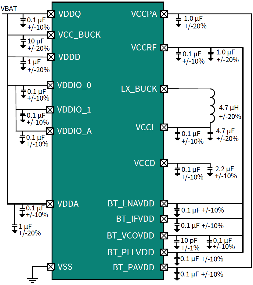
Figure 8 shows the typical connections for power pins for all supported packages. In the QFN packages, all internal grounds are routed to the metal pad (EPAD) in the package. This pad must be grounded on the PCB. Figure 8 shows 10 dBm PA configuration. For 0 dBm, connect BT_PAVDD to VCCRF.
Electrical specifications
All specifications are valid for -40°C < TA < 105°C and for 1.71 V to 3.6 V except where noted.
Absolute maximum ratings
| Spec ID# | Parameter | Description | Min | Typ | Max | Unit | Details/conditions |
|---|---|---|---|---|---|---|---|
| SID1 | VDD_ABS | Analog or digital supply relative to VSS (VSSD = VSSA) | –0.5 | - | 4 | V | Absolute maximum |
| SID2 | VCCD_ABS | Direct digital core voltage input relative to VSSD | –0.5 | - | 1.2 | V | Absolute maximum |
| SID3 | VGPIO_ABS | GPIO voltage; VDDD or VDDA | –0.5 | - | VDD + 0.5 | V | Absolute maximum |
| SID4 | IGPIO_ABS | Current per GPIO | –25 | - | 25 | mA | Absolute maximum |
| SID5 | IGPIO_injection | GPIO injection current per pin | –0.5 | - | 0.5 | mA | Absolute maximum |
| SID3A | ESD_HBM | Electrostatic discharge human body model | 2200 | - | – | V | Absolute maximum |
| SID4A | ESD_CDM | Electrostatic discharge charged device model | 500 | - | – | V | Absolute maximum |
| SID5A | LU | Pin current for latchup-free operation | –100 | - | 100 | mA | Absolute maximum |
| SIDWA8 | Vundershoot | Maximum undershoot voltage for I/O | - | - | –0.5 | V | Duration not to exceed 25% of the SIDWA9 V duty cycle |
| SIDWA9 | Vovershoot | Maximum overshoot voltage for I/O | - | - | VDDIO + 0.5 | V | Duration not to exceed 25% of the SIDWA9 V duty cycle |
| SIDWA10 | Tj | Maximum junction temperature | - | - | 125 | °C | – |
Operating conditions
| Spec ID# | Parameter | Description | Min | Typ | Max | Unit | Details/conditions |
|---|---|---|---|---|---|---|---|
| DC specifications | |||||||
| SID6 | VDDD | Internal regulator | 1.7 | - | 3.6 | V | - |
| SID7 | VDDA |
Analog power supply voltage. Shorted to VDDIO_A on PCB |
1.7 | - | 3.6 | V |
Internally unregulated supply |
| SID7M | MIC_BIAS | Microphone supply voltage | 1.7 | - | 3.6 | V |
Internally unregulated supply |
| SID7R | VCCI |
RF LDO and Digital LDO input. Connect to output of internal buck |
- | 1.16 | - | - | - |
| SID7C | |||||||
| SID7P | VDDD | PA LDO input | 2.7 | - | 3.6 | V |
For TX10 mode only, BT_PAVDD connected to VCCPA_0. The minimum supply voltage for VDDD has to be 2.7 V |
| SID7B | VDDIO_0 | GPIO supply for ports | 1.7 | - | 3.6 | V | - |
| SID7E | VDDIO_1 |
Supply when programming eFuse |
2.38 | 2.5 | 2.62 | V |
eFuse programming voltage |
| SID7A | VDDIO_A |
GPIO supply for analog ports. Short to VDDA on PCB |
1.7 | - | 3.6 | - | - |
| SID8 | VCCD (LP) |
Output voltage (for core logic bypass) |
- | 1.1 | - | V | High speed mode |
| SID9 | VCCD (ULP) |
Output voltage (for core logic bypass) |
- | 1.0 | - | V |
ULP mode. Valid for –40 to 105°C |
| SID10 | CEFC |
External regulator voltage (VCCD) bypass |
3.8 | 4.7 | 5.6 | µF |
X5R ceramic or better. Value for 0.8 to 1.2 V |
| SID11 | CEXC |
Power supply decoupling capacitor |
- | 10 | - | µF | X5R ceramic or better |
| SID12 | VCCRF | Output voltage (for radio) | - | 1.1 | - | V | - |
| SID13 | VCCPA | Output voltage (for PA) | - | 2.5 | - | V | - |
| SID523 | VDDQ | External supply to PMU analog | 1.7 | - | 3.6 | V | - |
| SID524 | VCC_BUCK |
External supply to switching regulator |
1.7 | - | 3.6 | V | - |
| SID525 | BT_PAVDD | Internal PA supply | 1 | - | 2.75 | V | - |
| SID526 | BT_RF | RF power supply | 1 | - | 1.2 | V | - |
| SID527 | BT_LNAVDD | LNA supply | 1 | - | 1.2 | V | - |
| SID528 | BT_IFVDD | IFPLL power supply | 1 | - | 1.2 | V | - |
| SID529 | BT_VCOVDD | VCO supply | 1 | - | 1.2 | V | - |
| CPU currents and transition times Cortex® M33 Active mode | |||||||
| Execute with cache enabled | |||||||
| SIDC2 | IDD4 |
Execute from cache; CM33 Active 96 MHz. FLL. Dhrystone |
- | 4.8 | 5.8 | mA |
VDDD = 3.0 V, Buck ON, Max at 60°C |
| - | 7.4 | 8.4 | mA |
VDDD = 1.8 V, Buck ON, Max at 60°C |
|||
| SIDC3 | IDD5 |
Execute from cache; CM33 Active 48 MHz. IHO. Dhrystone |
- | 2.4 | 3.4 | mA |
VDDD = 3.0 V, Buck ON, Max at 60°C |
| 3.7 | 4.1 | mA |
VDDD = 1.8 V, Buck ON, Max at 60°C |
||||
| SIDC4 | IDD6 |
Execute from cache; CM33 Active 8 MHz. IHO. Dhrystone |
- | 0.9 | 1.5 | mA |
VDDD = 3.0 V, Buck ON, Max at 60°C |
| 1.27 | 1.75 | mA |
VDDD = 1.8 V, Buck ON, Max at 60°C |
||||
| SIDS1 | IDD11 | CM33 Sleep 96 MHz with FLL | - | 1.5 | 2.2 | mA |
VDDD = 3.0 V, Buck ON, Max at 60°C |
| 2.2 | 2.7 | mA |
VDDD = 1.8 V, Buck ON, Max at 60°C |
||||
| SIDS2 | IDD12 | CM33 Sleep 48 MHz with IHO | - | 1.2 | 1.9 | mA |
VDDD = 3.0 V, Buck ON, Max at 60°C |
| 1.7 | 2.2 | mA |
VDDD = 1.8 V, Buck ON, Max at 60°C |
||||
| SIDS3 | IDD13 | CM33 Sleep 8 MHz with IHO | - | 0.7 | 1.3 | mA |
VDDD = 3.0 V, Buck ON, Max at 60°C |
| 0.96 | 1.5 | mA |
VDDD = 1.8 V, Buck ON, Max at 60°C |
||||
| Deep Sleep mode | |||||||
| SIDDS1_B | IDD33A_B |
With internal Buck enabled and 64K SRAM retention |
- | 5.7 | µA |
At 25°C (with typical Silicon) |
|
| SIDDS2_B | IDD33B_B |
With internal Buck enabled and 128K SRAM retention |
- | 6.2 | µA |
At 25°C (with typical Silicon) |
|
| SIDDS5_B | IDD33E_B |
With internal Buck enabled and 256K SRAM retention |
- | 7.5 | µA |
At 25°C (with typical Silicon) |
|
| SIDDS3_B | IDD33C_B |
With internal Buck enabled and 64K SRAM retention DS-RAM |
- | 4.5 | µA |
At 25°C (with typical Silicon) |
|
| SIDDS4_B | IDD33D_B |
With internal Buck enabled and 128K SRAM retention DS-RAM |
- | 5 | µA |
At 25°C (with typical Silicon) |
|
| SIDDS6_B | IDD33F_B |
With internal Buck enabled and 256K SRAM retention DS-RAM |
- | 6 | - | µA |
At 25°C (with typical Silicon) |
| Hibernate mode | |||||||
| SIDHIB1 | IDD34 | VDDD = 1.8 V | - | 300 | - | nA | No clocks running |
| SIDHIB2 | IDD34A | VDDD = 3.0 V | - | 500 | - | nA | No clocks running |
| SIDHIB3 | IDD35 | VDDD = 1.8 V | - | 800 | - | nA | WCO is running |
| SIDHIB4 | IDD35A | VDDD = 3.0 V | - | 1000 | - | nA | WCO is running |
| Power mode transition times | |||||||
| SID13A | TDS_ACT |
Deep Sleep to Active transition time. Guaranteed by design |
- | 45 | 60 | µs |
DS to Active with 1.0 V operation, with upper inrush current limit |
| SID13B | TDS_ACTLP |
Deep Sleep to Active LP transition time. Guaranteed by design |
- | 20 | 35 | µs |
DS to Active LP with 0.9 V operation |
| SID13C | TDSR_ACT |
Deep Sleep-RAM to Active transition time. Guaranteed by design |
- | - | 800 | µs |
DS to Active with 1.0 V operation, with upper inrush current limit |
| SID13D | TDSR_ACTLP |
Deep Sleep-RAM to Active LP transition time. Guaranteed by Design |
- | - | 800 | µs |
DS-RAM to Active LP with 0.9 V operation |
| SID14 | THIB_ACT |
Hibernate to Active transition time |
- | 2000 | - | µs |
Hibernate to Active with 1.0 V operation, with upper inrush current limit |
| SID14A | THIB_ACTLP |
Hibernate to Active LP transition time |
- | 2000 | - | µs |
Hibernate to Active with 0.9 V operation, with upper inrush current limit |
XRES
| Spec ID# | Parameter | Description | Min | Typ | Max | Unit | Details/conditions |
|---|---|---|---|---|---|---|---|
| SID17 | TXRES_IDD | IDD when XRES asserted | - | 300 | - | nA | VDDD = 1.8 V |
| SID17A | TXRES_IDD_1 | IDD when XRES asserted | - | 800 | - | nA | VDDD = 3.3 V |
| SID77 | VIH | Input voltage high threshold | 0.7 × VDD | - | - | V | CMOS input |
| SID78 | VIL | Input voltage low threshold | - | - | 0.3 × VDD | V | CMOS input |
| SID80 | CIN | Input capacitance | - | 3 | - | pF | - |
| SID81 | VHYSXRES | Input voltage hysteresis | - | 100 | - | mV | - |
| SID82 | IDIODE | Current through protection diode to VDD/VSS | - | - | 100 | µA | - |
| Spec ID# | Parameter | Description | Min | Typ | Max | Unit | Details/conditions |
|---|---|---|---|---|---|---|---|
| SID15 | TXRES_ACT | POR or XRES release to Active transition time | - | 1000 | - | µs | Normal mode, 96 MHz M33, upper inrush current |
| SID16 | TXRES_PW | XRES pulse width | 5 | - | - | µs | - |
GPIO
| Spec ID# | Parameter | Description | Min | Typ | Max | Unit | Details/conditions |
|---|---|---|---|---|---|---|---|
| SID57 | VIH | Input voltage HIGH threshold | 0.7 × VDD | - | - | V | CMOS input |
| SID57A | IIHS | Input current when Pad > VDDIO for OVT inputs | - | - | 10 | µA | Per I2C spec |
| SID58 | VIL | Input voltage LOW threshold | - | - | 0.3 × VDD | V | CMOS input |
| SID241 | VIH | LVTTL input, VDD < 2.7 V | 0.7 × VDD | - | - | V | - |
| SID242 | VIL | LVTTL input, VDD < 2.7 V | - | - | 0.3 × VDD | V | - |
| SID243 | VIH | LVTTL input, VDD > 2.7 V | 2.0 | - | - | V | - |
| SID244 | VIL | LVTTL input, VDD > 2.7 V | - | - | 0.8 | V | - |
| SID59 | VOH | Output voltage high level | VDD – 0.5 | - | - | V | IOH = 8 mA |
| SID62A | VOL | Output voltage low level | - | - | 0.4 | V | IOL = 8 mA |
| SID63 | RPULLUP | Pull-up resistor | 3.5 | 5.6 | 8.5 | kΩ | - |
| SID64 | RPULLDOWN | Pull-down resistor | 3.5 | 5.6 | 8.5 | kΩ | - |
| SID65 | IIL | Input leakage current (absolute value) | - | - | 2 | nA | 25°C, VDD = 3.0 V |
| SID66 | CIN | Input capacitance | - | - | 5 | pF | - |
| SID67 | VHYSTTL | Input hysteresis LVTTL VDD > 2.7 V | 100 | 0 | - | mV | - |
| SID68 | VHYSCMOS | Input hysteresis CMOS | 0.05 × VDD | - | - | mV | - |
| SID69 | IDIODE | Current through protection diode to VDD/VSS | - | - | 100 | µA | - |
| SID69A | ITOT_GPIO | Maximum total source or sink chip current | - | - | 200 | mA | - |
| Spec ID# | Parameter | Description | Min | Typ | Max | Unit | Details/conditions |
|---|---|---|---|---|---|---|---|
| SID70 | TRISEF | Rise time in Fast Strong mode. 10% to 90% of VDD | - | 3.5 | - | ns | CLOAD = 15 pF, 8 mA rive strength, VDDIO > 2.7 V |
| SID70A | TRISEF_1 | Rise time in Fast Strong mode. 10% to 90% of VDD | - | 5.5 | - | ns | CLOAD = 15pF, VDDIO < 2.7 V, maximum slew and drive strength |
| SID71 | TFALLF | Fall time in Fast Strong mode. 10% to 90% of VDD | - | 3.5 | - | ns | CLOAD = 15 pF, 8 mA drive strength, VDDIO > 2.7 V |
| SID71A | TFALLF_1 | Fall time in Fast Strong mode. 10% to 90% of VDD | - | 5.5 | - | ns | CLOAD = 15pF, VDDIO < 2.7 V, maximal slew and drive strength |
| SID72 | TRISES_1 | Rise time in Slow Strong mode. 10% to 90% of VDD | 52 | - | 142 | ns | CLOAD = 15 pF, 8 mA drive strength, VDD 2.7 V |
| SID72A | TRISES_2 | Rise time in Slow Strong mode. 10% to 90% of VDD | 48 | - | 102 | ns | CLOAD = 15 pF, 8 mA drive strength, 2.7 V < VDD 3.6 |
| SID73 | TFALLS_1 | Fall time in Slow Strong mode. 10% to 90% of VDD | 44 | - | 211 | ns | CLOAD = 15 pF, 8 mA drive strength, VDD 2.7 V |
| SID74 | FGPIOUT1 | GPIO Fout; Fast Strong mode | - | - | 100 | MHz | 90/10%, 15 pF load, 60/40 duty cycle |
| SID75 | FGPIOUT2 | GPIO Fout; Slow Strong mode | - | - | 1.5 | MHz | 90/10%, 15 pF load, 60/40 duty cycle |
| SID76 | FGPIOUT3 | GPIO Fout; Fast Strong mode | - | - | 100 | MHz | 90/10%, 15 pF load, 60/40 duty cycle |
| SID245 | FGPIOUT4 | GPIO Fout; Slow Strong mode | - | - | 1.3 | MHz | 90/10%, 15 pF load, 60/40 duty cycle |
| SID246 | FGPIOIN | GPIO input operating frequency; 1.71 V VDD 3.6 V | - | - | 100 | MHz | 90/10% VIO d |
Analog peripherals
| Spec ID# | Parameter | Description | Min | Typ | Max | Unit | Details/conditions |
|---|---|---|---|---|---|---|---|
| SID93R | VREFBG | - | 1.188 | 1.2 | 1.212 | V | - |
AUD ADC
| Spec ID# | Parameter | Description | Min | Typ | Max | Unit | Details/conditions |
|---|---|---|---|---|---|---|---|
| MIC specifications | |||||||
| DM.4 | - |
Audio/Mic supply - VDDA |
1.8 | - | 3.3 | V | - |
| DM.5 | - | Current consumption | - | 1.5 | - | mA |
25°C, VDDA = 3 V, excludes MIC_BIAS loading current |
| DM.6 | - | Power down current | - | 0.1 | - | µA | 25°C, VDDA = 3 V |
| DM.21 | - | MIC PGA gain range | 0 | - | 42 | dB | - |
| DM.22 | - | MIC PGA gain step | - | 1 | - | dB | - |
| DM.23 | - | MIC PGA gain error | - | ±1 | - | dB | - |
| DM.24 | - | PGA input referred noise | - | - | 4 | µV |
@ 42 dB PGA gain A-weighted |
| DM.25 | - | Passband gain flatness | - | - | - | dB | PGA + ADC, 100-4 kHz |
| DM.26 | - |
MIC_BIAS output voltage - VDDA * 0.75 * 1.12 |
- | 2.52 | - | V | VDDA = 3 V |
| DM.27 | - | MIC_BIAS loading current | - | - | 3 | mA | - |
| DM.28 | - | MIC_BIAS noise | - | - | 3 | µV |
Referred to PGA input, 20-8 kHz, A-weighted |
| DM.29 | - | MIC_BIAS PSRR | 40 | - | - | dB | 1 kHz |
| Spec ID# | Parameter | Description | Min | Typ | Max | Unit | Details/conditions |
|---|---|---|---|---|---|---|---|
| DM.2 | - | Analog supply voltage - VDDA | 1.7 | - | 3.6 | V | - |
| DM.5 | - | Active current consumption | - | 2 | - | mA | 25°C |
| DM.6 | - | Power down current | - | 0.1 | - | µA | 25°C - ADC disabled with device in Active mode |
| DM.8 | - | Absolute error - Includes gain error, offset and distortion | - | - | 5 | % | - |
| DM.10 | - | ENOB - Audio application | - | 12 | - | Bit | - |
| DM.11 | - | ENOB - Static application | - | 11 | - | Bit | - |
| DM.12 | - | ADC input full scale - Audio application |
- | 1.6 | - | Vpp | - |
| DM.13 | - | ADC input full scale - Static application |
0 | - | VDDA | Vpp | - |
| DM.14 | - | Conversion rate - Audio application |
16 | 48 | - | kHz | - |
| DM.15 | - | Conversion rate - Static application |
50 | 100 | - | kHz | - |
| DM.16 | - | Signal bandwidth - Audio application |
20 | - | 8000 | Hz | - |
| DM.17 | - | Signal bandwidth - Static application |
- | DC | - | Hz | - |
| DM.18 | - |
Startup time - Audio application |
- | 10 | - | ms | - |
| DM.19 | - |
Startup time - Static application |
- | 20 | - | µs | - |
| DM.30 | - | ADC SNR | 78 | - | - | dB |
0 dB PGA gain, A-weighted |
| DM.31 | - | ADC THD+N | 74 | - | - | dB |
–3 dB FS input, 0 dB PGA gain |
| DM.33 | - | GPIO source impedance | - | - | 1k | Ohm | 10 µs measurement time |
Digital peripherals
| Spec ID# | Parameter | Description | Min | Typ | Max | Unit | Details/conditions |
|---|---|---|---|---|---|---|---|
| SID.TCPWM.1 | ITCPWM1 |
Block current consumption at 8 MHz |
- | - | 70 | µA | All modes (TCPWM) |
| SID.TCPWM.2 | ITCPWM2 |
Block current consumption at 24 MHz |
- | - | 180 | µA | All modes (TCPWM) |
| SID.TCPWM.2A | ITCPWM3 |
Block current consumption at 50 MHz |
- | - | 270 | µA | All modes (TCPWM) |
| SID.TCPWM.2B | ITCPWM4 |
Block current consumption at 100 MHz |
- | - | 540 | µA | All modes (TCPWM) |
| SID.TCPWM.3 | TCPWMFREQ | Operating frequency | - | - | 100 | MHz |
Fc max = Fcpu Maximum = 100 MHz |
| SID.TCPWM.4 | TPWMENEXT |
Input trigger pulse width for all trigger events |
2/Fc | - | - | ns |
Trigger events can be Stop, Start, Reload, Count, Capture, or Kill depending on which mode of operation is selected |
| SID.TCPWM.5 | TPWMEXT |
Output trigger pulse widths |
1.5/Fc | - | - | ns |
Minimum possible width of Overflow, Underflow, and CC (Counter equals Compare value) trigger outputs |
| SID.TCPWM.5A | TCRES | Resolution of counter | 1/Fc | - | - | ns |
Minimum time between successive counts |
| SID.TCPWM.5B | PWMRES | PWM resolution | 1/Fc | - | - | ns |
Minimum pulse width of PWM output |
| SID.TCPWM.5C | QRES |
Quadrature inputs resolution |
2/Fc | - | - | ns |
Minimum pulse width between Quadrature phase inputs. Delays from pins should be similar |
| Spec ID# | Parameter | Description | Min | Typ | Max | Unit | Details/conditions |
|---|---|---|---|---|---|---|---|
| I2C DC specifications | |||||||
| SID149 | II2C1 | Block current consumption at 100 kHz | - | - | 30 | µA | - |
| SID150 | II2C2 | Block current consumption at 400 kHz | - | - | 80 | µA | - |
| SID151 | II2C3 | Block current consumption at 1 Mbps | - | - | 180 | µA | - |
| SID152 | II2C4 | I2C enabled in Deep
Sleep mode |
- | - | 1.7 | µA | At 60°C |
| I2C AC specifications | |||||||
| SID153 | FI2C1 | Bit rate | - | - | 1 | Mbps | - |
| UART DC specifications | |||||||
| SID160 | IUART1 | Block current consumption at 100 kbps | - | - | 30 | µA | - |
| SID161 | IUART2 | Block current consumption at 1000 kbps | - | - | 180 | µA | - |
| UART AC specifications | |||||||
| SID162A | FUART1 | Bit rate | - | - | 3 | Mbps | ULP mode |
| SID162B | FUART2 | Bit rate | - | - | 8 | Mbps | LP mode |
| SPI DC specifications | |||||||
| SID163 | ISPI1 | Block current consumption at 1 Mbps | - | - | 220 | µA | - |
| SID164 | ISPI2 | Block current consumption at 4 Mbps | - | - | 340 | µA | - |
| SID165 | ISPI3 | Block current consumption at 8 Mbps | - | - | 360 | µA | - |
| SID165A | ISP14 | Block current consumption at 25 Mbps | - | - | 800 | µA | - |
| SPI AC specifications for LP mode (VCCD = 1.1 V) unless noted otherwise | |||||||
| SID166 | FSPI | SPI operating frequency Master and externally clocked Slave | - | - | 24 | MHz | - |
| SID166B | FSPI_EXT | SPI operating frequency Master (Fscb is SPI clock) | - | - | Fscb/4 | MHz | Fscb max is 96 MHz in LP mode, 24 MHz in ULP mode |
| SID166A | FSPI_IC | SPI Slave internally clocked | - | - | 24 | MHz | - |
| SPI AC specifications for ULP mode (VCCD = 1.0 V) unless noted otherwise | |||||||
| SID166C | FSPI | SPI operating frequency Master and externally clocked Slave | - | - | 12 | MHz | - |
| SID166D | FSPI_EXT | SPI operating frequency Master (Fscb is SPI clock) | - | - | Fscb/4 | MHz | Fscb max is 48 MHz in ULP mode |
| SID166E | FSPI_IC | SPI Slave internally clocked | - | - | 12 | MHz | - |
| SPI Master mode AC specifications for LP mode (VCCD = 1.1 V) unless noted otherwise | |||||||
| SID167 | TDMO | MOSI valid after SClock driving edge | - | 12 | 12 | ns | 20 ns max. for ULP (VCCD=1.0 V) mode |
| SID168 | TDSI | MISO valid before SClock capturing edge | 20 | - | - | ns | Full clock, late MISO sampling |
| SID169 | THMO | MOSI data hold time | 0 | - | 5 | ns | Referred to Slave capturing edge |
| SID169C | TDHI | SPI Master: MISO hold time after SCLK capturing edge | 0 | - | - | ns | - |
| SID169A | TSSELMSCK1 | SSEL valid to first SCK valid edge | 18 | 21 | - | ns | Referred to Master clock edge |
| SPI Master mode AC specifications for ULP mode (VCCD = 1.0 V) unless noted otherwise | |||||||
| SID167A | TDMO | MOSI valid after SClock driving edge | - | - | 26 | ns | - |
| SID167B | TDSI | MISO valid before SClock capturing edge | 35 | - | - | ns | - |
| SID167C | THMO | MOSI data hold time | - | 5 | - | ns | - |
| SID167D | TDHI | SPI Master: MISO hold time after SCLK capturing edge | 0 | - | - | ns | - |
| SID167E | TSSELMSCK1 | SSEL valid to first SCK valid edge | 41 | - | - | ns | - |
| SPI Slave mode AC specifications for LP mode (VCCD = 1.1 V) unless noted otherwise | |||||||
| SID170 | TDMI | MOSI valid before Sclock capturing edge | 5 | - | - | ns | - |
| SID170A | SPI_FREQ | For LP mode | 48 | - | - | MHz | - |
| SID171A | TDSO_EXT | MISO valid after Sclock driving edge in Ext. Clk. mode | - | - | 20 | ns | 35 ns max. for ULP (VCCD=1.0V) mode |
| SID171 | TDSO | MISO valid after Sclock driving edge in Internally Clk. Mode | - | - |
TDSO_EXT + 3*Tscb |
ns |
Tscb is Serial Communication Block clock period |
| SID171B | TDSO | MISO valid after Sclock driving edge in Internally Clk. Mode with median filter enabled | - | - |
TDSO_EXT + 4*Tscb |
ns |
Tscb is Serial Communication Block clock period |
| SID172 | THSO | Previous MISO data hold time | 5.5 | - | - | ns | - |
| SID172C | THIS | SPI MOSI hold from SCLK | 5.5 | - | - | ns | - |
| SPI Slave mode AC specifications for ULP mode (VCCD = 1.0 V) unless noted otherwise | |||||||
| SID173A | TDMI | MOSI valid before Sclock capturing edge | 12 | - | - | ns | - |
| SID174A | TDSO_EXT | MISO valid after Sclock driving edge in Ext. Clk. mode | - | - | 20 | ns | - |
| SID174 | TDSO | MISO valid after Sclock driving edge in Internally Clk. Mode | - | - | TDSO_EXT + 3*Tscb | ns | - |
| SID174B | TDSO | MISO valid after Sclock driving edge in Internally Clk. Mode with median filter enabled | - | - | TDSO_EXT + 4*Tscb | ns | - |
| SID175 | THSO | Previous MISO data hold time | 5.5 | - | - | ns | - |
| SID175C | THIS | SPI MOSI hold from SCLK | 5.5 | - | - | ns | - |
Audio subsystem
| Spec ID# | Parameter | Description | Min | Typ | Max | Unit | Details/conditions |
|---|---|---|---|---|---|---|---|
| PDM specifications | |||||||
| SID400P | Fmax_clk_sys | Clock frequency for clk_sys | - | 96 | - | MHz | PVT18 ss, 0.90 V, –40°C, scl40 library, minimum parameters |
| SID401 | Fmax_clk_if_srss | Clock frequency for audio clock reference clk_if_srss | - | 48 | - | MHz | PVT18 ss, 0.90 V, –40°C, scl40 library, minimum parameters |
| SID402 | Idyn_act_typ | Typical dynamic current when cell is active. See the DC spec table for related static current spec, if applicable | - | - | 110 | µA/MHz | PVT16 tt, 1.1 V, 25°C, scl40 library, typical parameters clk_audio: 49.152 MHz clk_sys: 50 MHz |
| SID403 | Idyn_act_max | Maximum dynamic active current. See the DC spec table for related static current spec, if applicable | - | - | 132 | µA/MHz | PVT20 ff, 1.21 V, 150°C, scl40 library, maximum parameters clk_audio: 49.152 MHz clk_sys: 50 MHz |
| SID403A | Idyn_slp_typ | Typical dynamic current when cell is idle. See the DC spec table for related static current spec, if applicable | - | - | 80 | µA/MHz | PVT16 tt, 1.1 V, 25°C, scl40 library, typical parameters, clocks toggling clk_audio: 49.152 MHz clk_sys: 50 MHz |
| SID403B | T_SETUP | Receiver setup | - | - | 10 | ns | PVT18 ss, 0.90 V, –40°C, scl40 library, minimum parameters |
| SID403C | PDM_HOLD | Data input hold time to PDM_CLK edge | 10 | - | - | ns | PVT18 ss, 0.90 V, –40°C, scl40 library, minimum parameters |
| SID404A | CPDM | Load | - | 10 | - | pF | - |
| SID404 | PDM_OUT | Audio sample rate | 8 | - | 48 | ksps | - |
| SID405 | PDM_WL | Word length | 16 | - | 24 | bits | - |
| SID412 | PDM_ST | Startup time | - | 48 | - | - | WS (Word Select) cycles |
| I2S specifications. The same for LP and ULP modes unless stated otherwise. | |||||||
| SID413 | I2S_WORD | Length of I2S word | 8 | - | 32 | bits | - |
| SID414B | I2S_BCK_F | Bit Clock frequency in LP mode | - | - | 12.288 | MHz | - |
| SID414BU | I2S_BCK_F_U | Bit Clock frequency in ULP mode | - | - | 3.072 | MHz | - |
| SID414BP | I2S_BCK_P | Bit Clock period | - | 1/I2S_B CK_F | - | - | - |
| SID414BPU | I2S_BCK_P_U | Bit Clock period in ULP mode | - | 1/I2S_B CK_F_U | - | - | - |
| SID414 | I2S_WS_FREQ | Word clock frequency in LP mode | - | - | 192 | kHz | - |
| SID414M | I2S_WS_FREQ_U | Word clock frequency in ULP mode | - | - | 48 | kHz | - |
| SID435L | I2S_BCK_TL | Bit clock low period in LP Mode | 0.35*I2 S_BCK_ P | - | - | - | - |
| SID415IL | I2S_MCKI_TL | Master clock IN low period in LP (or) ULP mode | 0.45*tM CLK | - | - | - | - |
| SID415IH | I2S_MCKI_TH | Master clock IN high period in LP (or) ULP Mode | 0.45*tM CLK | - | - | - | - |
| SID415OL | I2S_MCKO_TL | Master clock Out low period in LP (or) ULP mode | 0.35*tM CLK | 0.45*t MCLK to 0.4*tMC LK | - | - | - |
| SID415OH | I2S_MCKO_TH | Master clock Out high period in LP (or) ULP mode | 0.35*tM CLK | 0.45*t MCLK to 0.4*tMC LK | - | - | - |
| SID416 | TDM_OUTPUT_LOAD_MAX | Capacitive load | 10 | - | - | - | - |
| I2S Slave mode | |||||||
| SID430 | I2S_S_TS_WS | WS Setup time before the first edge following the driving edge of Bit Clock for LP Mode | 0.2 * I2S_BC K_P | - | - | ns | - |
| SID430U | I2S_S_TS_WS_U | WS Setup time before the first edge following the driving edge of bit clock for ULP mode | 0.2 * I2S_BC K_P_U | - | - | ns | - |
| SID430A | I2S_S_TH_WS | WS Hold time after the first edge following the driving edge of bit clock, LP or ULP mode | 0 | - | - | ns | - |
| SID432 | I2S_S_SDO | SDO Propagation delay from driving edge of bit clock for LP mode | 0 | - | 0.3 * I2S_B CK_P | ns | - |
| SID432U | I2S_S_SDO_U | SDO Propagation delay from driving edge of bit clock for ULP mode | 0 | - | 0.3 * I2S_B CK_P | ns | - |
| I2S Master mode | |||||||
| SID437 | I2S_M_WS | WS propagation delay from driving edge of bit clock for LP mode | 0 | - | 0.2 * I2S_B CK_P | ns | - |
| SID437_U | I2S_M_WS_U | WS propagation delay from driving edge of bit clock for ULP mode | 0 | - | 0.2 * I2S_B CK_P _U | ns | - |
| SID438 | I2S_M_SDO | SDO Propagation delay from driving edge of bit clock for LP mode | 0 | - | 0.2 * I2S_B CK_P | ns | - |
| SID438U | I2S_M_SDO_U | SDO Propagation delay from driving edge of bit clock for ULP mode | 0 | - | 0.2 * I2S_B CK_P _U | ns | Associated clock edge depends on selected polarity |
System resources
Power-on reset
| Spec ID# | Parameter | Description | Min | Typ | Max | Unit | Details/conditions |
|---|---|---|---|---|---|---|---|
| Precise POR (PPOR) | |||||||
| SID190 | VFALLPPOR |
BOD trip voltage in Active and Sleep modes. VDDD |
1.54 | - | - | V | BOD Reset guaranteed for VDDD levels below 1.54 V |
| SID192 | VFALLDPSLP |
BOD trip voltage in Deep Sleep. VDDD |
1.54 | - | - | V | - |
| SID192A | VDDRAMP | Maximum power supply ramp rate (any supply) | - | - | 100 | mV/µs | Active mode |
| Spec ID# | Parameter | Description | Min | Typ | Max | Unit | Details/conditions |
|---|---|---|---|---|---|---|---|
| SID194A | VDDRAMP_DS | Maximum power supply ramp rate (any supply) in system Deep Sleep mode | - | - | 10 | mV/µs | BOD operation guaranteed |
Voltage monitors
| Spec ID# | Parameter | Description | Min | Typ | Max | Unit | Details/conditions |
|---|---|---|---|---|---|---|---|
| SID195 | VHVDI1 | - | 1.38 | 1.43 | 1.47 | V | - |
| SID196 | VHVDI2 | - | 1.57 | 1.63 | 1.68 | V | - |
| SID197 | VHVDI3 | - | 1.76 | 1.83 | 1.89 | V | - |
| SID198 | VHVDI4 | - | 1.95 | 2.03 | 2.10 | V | - |
| SID199 | VHVDI5 | - | 2.05 | 2.13 | 2.2 | V | - |
| SID200 | VHVDI6 | - | 2.15 | 2.23 | 2.3 | V | - |
| SID201 | VHVDI7 | - | 2.24 | 2.33 | 2.41 | V | - |
| SID202 | VHVDI8 | - | 2.34 | 2.43 | 2.51 | V | - |
| SID203 | VHVDI9 | - | 2.44 | 2.53 | 2.61 | V | - |
| SID204 | VHVDI10 | - | 2.53 | 2.63 | 2.72 | V | - |
| SID205 | VHVDI11 | - | 2.63 | 2.73 | 2.82 | V | - |
| SID206 | VHVDI12 | - | 2.73 | 2.83 | 2.92 | V | - |
| SID207 | VHVDI13 | - | 2.82 | 2.93 | 3.03 | V | - |
| SID208 | VHVDI14 | - | 2.92 | 3.03 | 3.13 | V | - |
| SID209 | VHVDI15 | - | 3.02 | 3.13 | 3.23 | V | - |
| SID211 | LVI_IDD | Block current | - | 5 | 15 | µA | - |
| Spec ID# | Parameter | Description | Min | Typ | Max | Unit | Details/conditions |
|---|---|---|---|---|---|---|---|
| SID212 | TMONTRIP | Voltage monitor trip time | - | - | 170 | nS | - |
SWD and trace interface
| Spec ID# | Parameter | Description | Min | Typ | Max | Unit | Details/conditions |
|---|---|---|---|---|---|---|---|
| SID214 | F_SWDCLK2 | 1.7 V ≤ VDDD ≤ 3.6 V | - | - | 25 | MHz | LP mode; VCCD = 1.1 V |
| SID214L | F_SWDCLK2L | 1.7 V ≤ VDDD ≤ 3.6 V | - | - | 12 | MHz | ULP mode; VCCD = 1.0 V. |
| SID215 | T_SWDI_SETUP | T = 1/f SWDCLK | 0.25 * T | - | - | ns | For both LP and ULP modes |
| SID216 | T_SWDI_HOLD | T = 1/f SWDCLK | 0.25 * T | - | - | ns | For both LP and ULP modes |
| SID217 | T_SWDO_VALID | T = 1/f SWDCLK | - | - | 0.5 * T | ns | - |
| SID217A | T_SWDO_HOLD | T = 1/f SWDCLK | 1 | - | - | ns | - |
| SID214T | F_TRCLK_LP1 | With trace data setup/hold times of 2/1 ns respectively | - | - | 48 | MHz | LP mode, VCCD = 1.1 V |
| SID215T | F_TRCLK_LP2 | With trace data setup/hold times of 3/2 ns respectively | - | - | 48 | MHz | LP mode, VCCD = 1.1 V |
| SID216T | F_TRCLK_ULP | With trace data setup/hold times of 3/2 ns respectively | - | - | 24 | MHz | ULP mode, VCCD = 1.0 V |
Internal main oscillator
| Spec ID# | Parameter | Description | Min | Typ | Max | Unit | Details/conditions |
|---|---|---|---|---|---|---|---|
| SID218 | IIMO1 | IMO operating current at 8 MHz | - | 9 | 15 | µA | - |
| Spec ID# | Parameter | Description | Min | Typ | Max | Unit | Details/conditions |
|---|---|---|---|---|---|---|---|
| SID223 | FIMOTOL1 | Frequency variation centered on 8 MHz | - | - | ±2 | % | - |
| SID227 | TJITR | Cycle-to-cycle and period jitter | - | ±250 | - | µs | - |
Internal low-speed oscillator
| Spec ID# | Parameter | Description | Min | Typ | Max | Unit | Details/conditions |
|---|---|---|---|---|---|---|---|
| SID231 | IILO2 | ILO operating current at 32 kHz | - | 0.3 | 0.7 | µA | - |
| Spec ID# | Parameter | Description | Min | Typ | Max | Unit | Details/conditions |
|---|---|---|---|---|---|---|---|
| SID234 | TSTARTILO1 | ILO startup time | - | - | 7 | µs |
Startup time to 80% of final frequency |
| - | - | 35 | µs | Startup time to 95% of final frequency | |||
| SID236 | TLIODUTY | ILO duty cycle | 45 | 50 | 55 | % | - |
| SID237 | FILOTRIM1 | 32 kHz trimmed frequency | 28.8 | 32 | 35.2 | kHz | ± 10% variations |
FLL
| Spec ID# | Parameter | Description | Min | Typ | Max | Unit | Details/conditions |
|---|---|---|---|---|---|---|---|
| SID450 | FLL_RANGE | Input frequency range | 0.040 | - | 96.00 | MHz | Upper limit is for External input |
| SID451 | FLL_OUT_DIV2 | Output frequency range. VCCD = 1.1 V | 24.00 | - | 96.00 | MHz | Output range of FLL divided by 2 output |
| SID451A | FLL_OUT_DIV2 | Output frequency range. VCCD = 0.9 V | 24.00 | - | 48.00 | MHz | Output range of FLL divided by 2 output |
| SID452 | FLL_DUTY_DIV2 | Divided-by-2 output; High or Low | 47.00 | - | 53.00 | % | - |
| SID454 | FLL_WAKEUP | Time from stable input clock to 1% of final value on deep sleep wakeup | - | - | 11.00 | µs | With IMO input, less than 10°C change in temperature while in Deep Sleep, and Fout 50 MHz. |
| SID455 | FLL_JITTER | Period jitter (1 sigma at 100 MHz) | - | - | 18.00 | ps | - |
| SID456 | FLL_CURRENT | CCO + logic current | - | - | 5.50 | µA/MHz | - |
Crystal oscillator
| Spec ID# | Parameter | Description | Min | Typ | Max | Unit | Details/conditions |
|---|---|---|---|---|---|---|---|
| MHz ECO DC specifications | |||||||
| SID316 | IDD_MHZ | Block operating current with Cload up to 18 pF | - | 1200 | - | µA | Type 24 MHz |
| MHz ECO AC specifications | |||||||
| SID317 | F_MHz | Crystal frequency range | - | 24 | - | MHz | - |
| kHz ECO DC specifications | |||||||
| SID318 | IDD_kHz | Block operating current with 32-kHz crystal | - | 0.38 | 1 | µA | - |
| SID321E | ESR32K | Equivalent series resistance | - | 80 | - | kΩ | - |
| SID322E | PD32K | Drive level | - | - | 0.5 | µW | - |
| kHz ECO AC specifications | |||||||
| SID319 | F_kHz | 32-kHz trimmed frequency | - | 32.8 | - | kHz | - |
| SID320 | Ton_kHz | Startup time | - | - | 1000 | ms | - |
| SID320E | FTOL32K | Frequency tolerance | - | 50 | 250 | ppm | - |
Clock source switching time
| Spec ID# | Parameter | Description | Min | Typ | Max | Unit | Details/conditions |
|---|---|---|---|---|---|---|---|
| SID262 | TCLKSWITCH | Clock switching from one CLK_HF to another CLK_HF in clock periods6 | - | - | 4 clk1 + 3 clk2 | periods | - |
QSPI
| Spec ID# | Parameter | Description | Min | Typ | Max | Unit | Details/conditions |
|---|---|---|---|---|---|---|---|
| SMIF QSPI specifications. All specs with 15-pF load | |||||||
| SID390Q | Fsmifclock | SMIF QSPI output clock frequency | - | - | 48 | MHz | LP mode (1.1 V) |
| SID390QU | Fsmifclocku | SMIF QSPI output clock frequency | - | - | 24 | MHz | ULP mode (1.0 V) |
| SID397Q | Idd_qspi | Block current in LP mode (1.0 V) | - | - | 1900 | µA | LP mode (1.1 V) |
| SID398Q | Idd_qspi_u | Block current in ULP mode (0.9 V) | - | - | 590 | µA | ULP mode (1.0 V) |
| SID399A | SDR_TCSH0 | CS# active hold to CK | 4 | - | - | ns | - |
| SID399B | SDR_TOUT_ SETUP_LF | Output setup time of DQ[3:0] to CK high | 5.1 | - | - | ns | - |
| SID399C | SDR_TOUT_ HOLD_LF | Output hold time of DQ[3:0] to CK high | 5.1 | - | - | ns | - |
| SID399D | SDR_TIN_V | CK low to DQ[3:0] input valid time | - | - | 6.7 | ns | - |
| SID399E | SDR_TIN_HO | CK low to DQ[3:0] input hold time | 1 | - | - | ns | - |
Smart I/O
| Spec ID# | Parameter | Description | Min | Typ | Max | Unit | Details/conditions |
|---|---|---|---|---|---|---|---|
| SID420 | SMIO_BYP | Smart I/O Bypass delay | - | - | 2 | ns | - |
| SID421 | SMIO_LUT | Smart I/O LUT prop delay | - | - | 2 | ns | - |
JTAG boundary scan
| Spec ID# | Parameter | Min | Typ | Max | Unit | Desctiption | |
|---|---|---|---|---|---|---|---|
| JTAG boundary scan parameters | |||||||
| SID460 | TCKLOW | TCK LOW minimum | 34 | - | - | ns | - |
| SID461 | TCKHIGH | TCK HIGH | 10 | - | - | ns | - |
| SID462 | TCK_TDO | TDO clock-to-out (max) from falling TCK | - | - | 22 | ns | - |
| SID463 | TSU_TCK | TDI, TMS Setup time before rising TCK | 12 | - | - | ns | - |
| SID464 | TCk_THD | TDI, TMS Hold time after rising TCK | 10 | - | - | ns | - |
| SID465 | TCK_TDOV | TCK to TDO data valid (High-Z to active) | 22 | - | - | ns | - |
| SID466 | TCK_TDOZ | TCK to TDO data valid (Active to High-Z) | 22 | - | - | ns | - |
| JTAG boundary scan parameters for 1.1 V (LP) mode operation | |||||||
| SID468 | TCKLOW | TCK low | 52 | - | - | ns | - |
| SID469 | TCKHIGH | TCK high | 10 | - | - | ns | - |
| SID469A | TCKPERIOD | CLK_JTAG_PERIOD, 30 pF load | - | 62 | - | ns | - |
| SID470 | TCK_TDO | TCK falling edge to output valid | - | - | 40 | ns | - |
| SID471 | TSU_TCK | Input valid to TCK rising edge | 12 | - | - | ns | - |
| SID472 | TCk_THD | Input hold time to TCK rising edge | 10 | - | - | ns | - |
| SID473 | TCK_TDOV | TCK falling edge to output valid (High-Z to active) | 40 | - | - | ns | - |
| JTAG boundary scan p for 1.0 V (ULP) mode operation | |||||||
| SID468A | TCKLOW | TCK low | 102 | - | - | ns | - |
| SID469A | TCKHIGH | TCK high | 20 | - | - | ns | - |
| SID470A | TCK_TDO | TCK falling edge to output valid | - | - | 80 | ns | - |
| SID471A | TSU_TCK | Input valid to TCK rising edge | 22 | - | - | ns | - |
| SID472A | TCk_THD | Input hold time to TCK rising edge | 20 | - | - | ns | - |
| SID473A | TCK_TDOV | TCK falling edge to output valid (High-Z to active) | 80 | - | - | ns | - |
| SID474A | TCK_TDOZ | TCK fallingedgetooutput valid (Active to high-Z) | 80 | - | - | ns | - |
Bluetooth® LE
| Spec ID# | Parameter | Description | Min | Typ | Max | Unit | Details/conditions |
|---|---|---|---|---|---|---|---|
| RF receiver specifications (1 Mbps) | |||||||
| SID317R | RXS, IDLE | RX sensitivity with ideal transmitter | - | -98 | - | dBm | Across RF operating frequency range |
| SID318R | RXS, IDLE | RX sensitivity with ideal transmitter | - | -96.5 | - | dBm | |
| SID319R | PRXMAX | Maximum received signal strength at < 30.8% PER | - | -5 | - | dBm |
RF-PHY specification (RCV-LE/CA/06/C) |
| SID320R | CI1 |
Co-channel interference, Wanted Signal at –67 dBm and Interferer at FRX |
- | 9 | 21 | dB |
RF-PHY specification (RCV-LE/CA/03/C) |
| SID321R | CI2 |
Adjacent channel interference Wanted Signal at –67 dBm and Interferer at FRX ± 1 MHz |
- | -3 | 15 | dB |
RF-PHY specification (RCV-LE/CA/03/C) |
| SID322R | CI3 |
Adjacent channel interference Wanted Signal at –67 dBm and Interferer at FRX ± 2 MHz |
- | -45 | -17 | dB |
RF-PHY specification (RCV-LE/CA/03/C) |
| SID323R | CI4 |
Adjacent channel interference Wanted Signal at –67 dBm and Interferer at ≥ FRX ± 3 MHz |
- | -49 | -27 | dB |
RF-PHY specification (RCV-LE/CA/03/C) |
| SID324R | CI5 |
Adjacent channel interference Wanted Signal at –67 dBm and Interferer at image frequency (FIMAGE) |
- | -31 | -9 | dB |
RF-PHY specification (RCV-LE/CA/03/C) |
| SID325R | CI6 |
Adjacent channel interference Wanted Signal at –67dBm and Interferer at image frequency (FIMAGE ± 1 MHz) |
- | -35 | -15 | dB |
RF-PHY specification (RCV-LE/CA/03/C) |
| RF receiver specifications (2 Mbps) | |||||||
| SID3267 | RXS, IDLE | RX sensitivity with ideal transmitter | - | -95 | - | dBm |
Across RF operating frequency range |
| SID3278 | RXS, IDLE | RX sensitivity with ideal transmitter | - | -93.5 | - | dBm | |
| SID328R | PRXMAX | Maximum received signal strength at < 30.8% PER | - | -5 | - | dBm |
RF-PHY specification (RCV-LE/CA/06/C) |
| SID329R | CI1 | Co-channel interference, Wanted Signal at –67 dBm and Interferer at FRX | - | 7 | 21 | dB |
RF-PHY specification (RCV-LE/CA/03/C) |
| SID330 | CI2 | Adjacent channel interference Wanted Signal at –67 dBm and Interferer at FRX ± 2 MHz | - | -2 | 15 | dB |
RF-PHY specification (RCV-LE/CA/03/C) |
| SID331 | CI3 | Adjacent channel interference Wanted Signal at –67 dBm and Interferer at FRX ± 4 MHz | - | -42 | -15 | dB |
RF-PHY specification (RCV-LE/CA/03/C) |
| SID332 | CI4 | Adjacent channel interference Wanted Signal at –67 dBm and Interferer at ≥ FRX ± 6 MHz | - | -42 | -27 | dB |
RF-PHY specification (RCV-LE/CA/03/C) |
| SID333 | CI5 | Adjacent channel interference Wanted Signal at –67 dBm and Interferer at Image frequency (FIMAGE) | - | -29 | -9 | dB |
RF-PHY specification (RCV-LE/CA/03/C) |
| SID334 | CI6 | Adjacent channel interference Wanted Signal at –67 dBm and Interferer at Image frequency (FIMAGE ± 2 MHz) | - | -40 | -15 | dB |
RF-PHY specification (RCV-LE/CA/03/C) |
| RF receiver specification S2 (500 kbps) | |||||||
| SID501 | RXS, IDLE | RX sensitivity with Ideal Transmitter, Standard Mod Index Rx | - | -101 | - | dBm | Across RF operating frequency range |
| SID506 | CI1 | Co-channel interference, Wanted Signal at –72 dBm and Interferer at FRX | - | 3 | 17 | dB | RF-PHY specification (RCV-LE/CA/28/C) |
| SID507 | CI2 | Adjacent channel interference Wanted Signal at –72 dBm and Interferer at FRX ± 1 MHz | - | -11 | 11 | dB | RF-PHY specification (RCV-LE/CA/28/C) |
| SID508 | CI3 | Adjacent channel interference Wanted Signal at –72 dBm and Interferer at FRX ± 2 MHz | - | -50 | -21 | dB | RF-PHY specification (RCV-LE/CA/28/C) |
| SID509 | CI4 | Adjacent channel interference Wanted Signal at –72 dBm and Interferer at FRX ± 3 MHz | - | -53 | -31 | dB | RF-PHY specification (RCV-LE/CA/28/C) |
| SID510 | CI5 | Adjacent channel interference Wanted Signal at –72 dBm and Interferer at image frequency (FIMAGE) | - | -37 | -13 | dB | RF-PHY specification (RCV-LE/CA/28/C) |
| SID511 | CI6 | Adjacent channel interference Wanted Signal at –72 dBm and Interferer at image frequency (FIMAGE ± 1 MHz) | - | -42 | -19 | dB | RF-PHY specification (RCV-LE/CA/28/C) |
| RF Receiver specification S8 (125 kbps) | |||||||
| SID512 | RXS, IDLE | RX sensitivity with Ideal Transmitter8 | - | -106 | - | dBm | Across RF operating frequency range |
| SID517 | CI1 | Co-channel interference, Wanted Signal at –79 dBm and Interferer at FRX | - | 6 | 12 | dB | RF-PHY specification (RCV-LE/CA/29/C) |
| SID518 | CI2 | Adjacent channel interference Wanted Signal at –79 dBm and Interferer at FRX ± 1 MHz | - | -18 | 6 | - | RF-PHY specification (RCV-LE/CA/29/C) |
| SID519 | CI3 | Adjacent channel interference Wanted Signal at –79 dBm and Interferer at FRX ± 2 MHz | - | -52 | -26 | - | RF-PHY specification (RCV-LE/CA/29/C) |
| SID520 | CI4 | Adjacent channel interference Wanted Signal at –79 dBm and Interferer at FRX ± 3 MHz | - | -51 | 36 | - | RF-PHY specification (RCV-LE/CA/29/C) |
| SID521 | CI5 | Adjacent channel interference Wanted Signal at –79 dBm and Interferer at Image frequency (FIMAGE) | - | -40 | -18 | - | RF-PHY specification (RCV-LE/CA/29/C) |
| SID522 | CI6 | Adjacent channel interference Wanted Signal at –79 dBm and Interferer at Image frequency (FIMAGE ± 1 MHz) | - | -47 | -24 | - | RF-PHY specification (RCV-LE/CA/29/C) |
| RF Receiver specification (1 and 2 Mbps) | |||||||
| SID338 | OBB1 | Out of Band Blocking Wanted Signal at –67 dBm and Interferer at F = 30 –2000 MHz | -30 | - | - | dBm | RF-PHY specification (RCV-LE/CA/04/C) |
| SID339 | OBB2 | Out of Band Blocking Wanted Signal at –67 dBm and Interferer at F = 2003 - 2399 MHz | -35 | - | - | dBm | RF-PHY specification (RCV-LE/CA/04/C) |
| SID340 | OBB3 | Out of Band Blocking, Wanted Signal at –67 dBm and Interferer at F = 2484 - 2997 MHz | -35 | - | - | dBm | RF-PHY specification (RCV-LE/CA/04/C) |
| SID341 | OBB4 | Out of Band Blocking Wanted Signal at -67 dBm and Interferer at F = 3000 - 12750 MHz | -30 | - | - | dBm | RF-PHY specification (RCV-LE/CA/04/C) |
| SID342 | IMD | Intermodulation Performance Wanted Signal at –64 dBm and 1 Mbps Bluetooth® LE, 3rd, 4th and 5th offset channel | -50 | - | - | dBm | RF-PHY specification (RCV-LE/CA/05/C) |
| SID343 | RXSE1 | Receiver Spurious emission 30 MHz to 1.0 GHz | - | - | -57 | dBm | 100 kHz measurement bandwidth ETSI EN300 328 V2.1.1 |
| SID344 | RXSE2 | Receiver Spurious emission 1.0 GHz to 12.75 GHz | - | - | -53 | dBm | 1 MHz measurement bandwidth ETSI EN300 328 V2.1.1 |
| RF Transmitter specifications | |||||||
| SID345 | TXP, ACC | RF power accuracy | -2 | - | 2 | dB | - |
| SID346 | TX0 | Power range | - | 23 | - | dB | –24 dBm to 0 dBm |
| TX10 | Power range | - | 33 | - | dB | –24 dBm to 10 dBm | |
| SID347 | TXP, 0 dBm | Output power, 0 dB power setting | - | 0 | - | dBm | For TX10 mode, BT_PAVDD connected to VCCPA_0. The minimum supply voltage VDDD is 2.7 V |
| SID348 | TXP, 10 dBm | Output power, 10 dBm power setting | - | 10 | - | dBm | For TX10 mode, BT_PAVDD connected to VCCPA_0. The minimum supply voltage VDDD is 2.7 V |
| SID349 | TXP, MIN | Output power, minimum power setting | - | -20 | - | dBm | For TX10 mode, BT_PAVDD connected to VCCPA_0. The minimum supply voltage VDDD is 2.7 V |
| SID350 | F2Max | Average frequency deviation for 10101010 pattern | 185 | - | - | kHz | RF-PHY specification (TRM-LE/CA/05/C) |
| SID350R | F2Max_2M | Average frequency deviation for 10101010 pattern for 2 Mbps | 370 | - | - | kHz | RF-PHY specification (TRM-LE/CA/05/C) |
| SID350LR | F1Max_S8 | Average frequency deviation for 10101010 pattern for 125 bps | 185 | - | - | kHz | RF-PHY specification (TRM-LE/CA/13/C) |
| SID351 | F1AVG | Average frequency deviation for 11110000 pattern | 225 | 250 | 275 | kHz | RF-PHY specification (TRM-LE/CA/05/C) |
| SID351R | F1AVG_2M | Average frequency deviation for 11110000 pattern for 2 Mbps | 450 | 500 | 550 | kHz | RF-PHY specification (TRM-LE/CA/05/C) |
| SID351R | F1AVG_S8 | Average frequency deviation for 11110000 pattern for 125 kbps | 225 | 250 | 275 | kHz | RF-PHY specification (TRM-LE/CA/13/C) |
| SID352 | EO | Eye opening = ∆F2AVG/∆F1AVG | 0.8 | - | - | - | RF-PHY specification (TRM-LE/CA/05/C) |
| SID353 | FTX,ACC | Frequency accuracy | -150 | - | 150 | kHz | RF-PHY specification (TRM-LE/CA/06/C) |
| SID354 | FTX,MAXDR | Maximum frequency drift | -50 | - | 50 | kHz | RF-PHY specification (TRM-LE/CA/06/C) |
| SID355 | FTX, INITDR | Initial frequency drift | -20 | - | 20 | kHz | RF-PHY specification (TRM-LE/CA/06/C) |
| SID355LR | FTX, INITDR, S8 | Initial frequency drift | -19.2 | - | 19.2 | kHz | RF-PHY specification (TRM-LE/CA/14/C) |
| SID356 | FTX, DR | Maximum drift rate | -20 | - | 20 |
kHz/ 50 µs |
RF-PHY specification (TRM-LE/CA/06/C) |
| FTX, DR, S8 | Maximum drift rate | -19.2 | - | 19.2 |
kHz/ 50 µs |
RF-PHY specification (TRM-LE/CA/14/C) | |
| SID357 | IBSE1 |
In Band Spurious Emission at 2 MHz offset (1 Mbps) In Band Spurious Emission at 4 MHz offset (2 Mbps) |
- | - | -20 | dBm | RF-PHY specification (TRM-LE/CA/03/C) |
| SID358 | IBSE2 | In Band Spurious Emission at > 3 MHz offset (1
Mbps) In Band Spurious Emission at > 6 MHz offset (2 Mbps) |
- | - | -30 | dBm | RF-PHY specification (TRM-LE/CA/03/C) |
| SID359 | TXSE1 | Transmitter Spurious Emissions (Averaging), < 1.0 GHz | - | - | -55.5 | dBm | FCC-15.247 |
| SID360 | TXSE2 | Transmitter Spurious Emissions (Averaging), > 1.0 GHz |
- | - | -41.5 | dBm | FCC-15.247 |
| RF Current specifications | |||||||
| SID361 | IRX1_wb | Receive current (LE 1 Mbps) | - | 5.6 | - | mA | Measured with VCC_BUCK = 3.0 V. In all cases, VCCI = 1.16 V and VCCRF = 1.1 V. For TX0, BT_PAVDD = VCCRF. For TX10, BT_PAVDD = VCCPA_0 = 2.5 V |
| SID362 | ITX1_0dBm | TX current at 0 dBm setting (LE 1 Mbps) | - | 5.2 | - | mA | |
| SID365R | ITX1_10dBm | TX current at 10 dBm setting (LE 1 Mbps) | - | 17.2 | - | mA | |
| General RF specifications | |||||||
| SID373 | FREQ | RF operating frequency | 2402 | - | 2480 | MHz | - |
| SID374 | CHBW | Channel spacing | - | 2 | - | MHz | - |
| SID375 | DR1 | On-air data rate (1 Mbps) | - | 1000 | - | kbps | - |
| SID376 | DR2 | On-air data rate (2 Mbps) | - | 2000 | - | kbps | - |
| RSSI specifications | |||||||
| SID379 | RSSI, ACC | RSSI accuracy | -4 | - | 4 | dB | –95 dBm to –20 dBm measurement range |
| SID380 | RSSI, RES | RSSI resolution | - | 1 | - | dB | |
| SID381 | RSSI, PER | RSSI sample period | - | 6 | - | µs | – |
| System-level Bluetooth® LE specifications | |||||||
| SID433R | Adv_Pwr |
Advertising power, 1.28 s advertising interval, 31 bytes, TX 0 dBm |
- | 44.5 | - | µW | Connectible advertising, VBAT = 3.0 V. Measured with WCO. |
| - | 46.9 | - | µW | Connectible advertising, VBAT = 3.0 V. Measured with PILO. | |||
| SID434R |
Conn_Pwr_300 |
Connection power, 300 ms connection interval, 0 bytes, TX 0 dBm |
- | 64.6 | - | µW | VBAT = 3.0 V. Measured with WCO. |
| - | 68.0 | - | µW | VBAT = 3.0 V. Measured with PILO. | |||
| SID435R | Conn_Pwr_1S |
Connection power, 1000 ms connection interval, 0 bytes, TX 0 dBm |
- | 29.5 | - | µW | VBAT = 3.0 V. Measured with WCO. |
| - | 32.4 | - | µW | VBAT = 3.0 V. Measured with PILO. | |||
Ordering information
Table 38 lists the CYW20829 part numbers and features.
| Product | Description | Package | Ambient operating temperature |
|---|---|---|---|
| CYW20829B1000 | Entry level consumer focus product | 6 6 0.9 mm 56-lead | -40°C to 105°C |
| CYW20829B10109 | Full featured consumer focus product with LE Audio and Automotive peripherals | 6 6 0.9 mm 56-lead | -40°C to 105°C |
Packaging
This product line is offered in 56-lead package.
| Spec ID# | Package | Description | Package drawing number |
|---|---|---|---|
| PKG_2 | 56-lead | 56-lead, 6 6 0.9 mm height with 0.35-mm pitch | 002-31757 |
| Parameter | Description | Conditions | Min | Typ | Max | Unit |
|---|---|---|---|---|---|---|
| TA | Operating ambient | - | -40 | 25 | 105 | °C |
| TJ | Operating junction | - | - | 105 | °C | |
| TJA | Package JA (56-lead) | - | - | 13.8 | - | °C/watt |
| TJC | Package JC (56-lead) | - | - | 4.8 | - | °C/watt |
| Package | Maximum peak temperature | Maximum time at peak temperature |
|---|---|---|
| 56-lead | 260°C | 30 s |
| Package | MSL |
|---|---|
| 56-lead | MSL-3 |
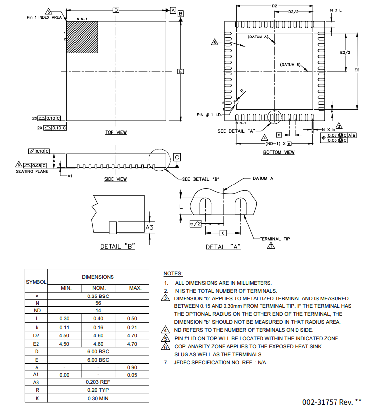
Acronyms
| Acronym | Description |
|---|---|
| 3DES | triple DES (data encryption standard) |
| ADC | analog-to-digital converter |
| AES | advanced encryption standard |
| AHB | AMBA (advanced microcontroller bus architecture) high-performance bus, an Arm® data transfer bus |
| API | application programming interface |
| Arm® | advanced RISC machine, a CPU architecture |
| BOD | brown-out detect |
| BTSS | Bluetooth® sub system |
| CAD | computer aided design |
| CBC | cipher block chaining |
| CFB | cipher feedback |
| CCO | current controlled oscillator |
| CM0+ | Cortex®-M0+, an Arm® CPU |
| CM4 | Cortex®-M4, an Arm® CPU |
| CMOS | complementary metal-oxide-semiconductor, a process technology for IC fabrication |
| CPU | central processing unit |
| CRC | cyclic redundancy check, an error-checking protocol |
| CSD | CAPSENSE™ sigma-delta |
| CTR | Counter |
| DAC | digital-to-analog converter, see also IDAC, VDAC |
| DAP | debug access port |
| DES | data encryption standard |
| DMA | direct memory access, see also TD |
| DNL | differential nonlinearity, see also INL |
| DSI | digital system interconnect |
| ECB | electronic code book |
| ECC | elliptic curve cryptography |
| ECDSA | elliptic curve digital signature algorithm |
| ECO | external crystal oscillator |
| EMI | electromagnetic interference |
| ESD | electrostatic discharge |
| FIFO | first-in, first-out |
| FLL | frequency locked loop |
| FS | full-speed |
| GND | Ground |
| GPIO | general-purpose input/output |
| HMAC | hash-based message authentication code |
| HSIOM | high-speed I/O matrix |
| I/O | input/output, see also GPIO, DIO, SIO, USBIO |
| I2C, or IIC | Inter-Integrated Circuit, a communications protocol |
| I2S | inter-IC sound |
| IC | integrated circuit |
| IDAC | current DAC, see also DAC, VDAC |
| IDE | integrated development environment |
| ILO | internal low-speed oscillator, see also IMO |
| IMO | internal main oscillator, see also ILO |
| INL | integral nonlinearity, see also DNL |
| IoT | internet of things |
| IPC | inter-processor communication |
| IRQ | interrupt request |
| JTAG | Joint Test Action Group |
| LIN | Local Interconnect Network, a communications protocol |
| LP | low power |
| LS | low-speed |
| LUT | lookup table |
| LVD | low-voltage detect, see also LVI |
| LVTTL | low-voltage transistor-transistor logic |
| MAC | multiply-accumulate |
| MCU | microcontroller unit |
| MCWDT | multi-counter watchdog timer |
| MISO | master-in slave-out |
| MMIO | memory-mapped input output |
| MOSI | master-out slave-in |
| MPU | memory protection unit |
| MSL | moisture sensitivity level |
| NMI | nonmaskable interrupt |
| NVIC | nested vectored interrupt controller |
| OFB | output feedback |
| OTP | one-time programmable |
| OVT | overvoltage tolerant |
| PCB | printed circuit board |
| PCM | pulse code modulation |
| PDM | pulse density modulation |
| PHY | physical layer |
| PLL | phase-locked loop |
| POR | power-on reset |
| PRNG | pseudo random number generator |
| PSRR | power supply rejection ratio |
| PWM | pulse-width modulator |
| QD | quadrature decoder |
| QSPI | quad serial peripheral interface |
| RAM | random-access memory |
| RISC | reduced-instruction-set computing |
| ROM | read-only memory |
| RTC | real-time clock |
| RX | receive |
| SAR | successive approximation register |
| SARMUX | SAR ADC multiplexer bus |
| SCB | serial communication block |
| SHA | secure hash algorithm |
| SMIF | serial media interface |
| SNR | signal-to-noise ration |
| SPI | Serial Peripheral Interface, a communications protocol |
| SRAM | static random access memory |
| SROM | supervisory read-only memory |
| SWD | serial wire debug, a test protocol |
| SWJ | serial wire JTAG |
| SWO | single wire output |
| SWV | serial-wire viewer |
| TCPWM | timer, counter, pulse-width modulator |
| TDM | time division multiplexed |
| TRNG | true random number generator |
| TX | transmit |
| UART | Universal Asynchronous Transmitter Receiver, a communications protocol |
| ULP | ultra-low power |
| WCO | watch crystal oscillator |
| WDT | watchdog timer |
| WIC | wakeup interrupt controller |
| XIP | execute-in-place |
| XRES | external reset input pin |
Document conventions
Units of measure
| Symbol | Unit of measure |
|---|---|
| °C | degrees celsius |
| dB | decibel |
| fF | femto farad |
| Hz | hertz |
| KB | 1024 bytes |
| kbps | kilobits per second |
| khr | kilohour |
| kHz | kilohertz |
| kΩ | kilo ohm |
| ksps | kilosamples per second |
| LSb | least significant bit |
| Mbps | megabits per second |
| MHz | megahertz |
| MΩ | mega-ohm |
| Msps | megasamples per second |
| µA | microampere |
| µF | microfarad |
| µH | microhenry |
| µs | microsecond |
| µV | microvolt |
| µW | microwatt |
| mA | milliampere |
| ms | millisecond |
| mV | millivolt |
| nA | nanoampere |
| ns | nanosecond |
| nV | nanovolt |
| W | ohm |
| pF | picofarad |
| ppm | parts per million |
| ps | picosecond |
| s | second |
| sps | samples per second |
| sqrtHz | square root of hertz |
| V | volt |
Revision history
| Document version | Date of release | Description of changes |
|---|---|---|
| *H | 2024-04-09 |
Updated the doc status to Final. Updated Bluetooth® Low Energy subsystem and added a footnote. Updated the part number: CYW20829B0LKMLTXUMA1/CYW20829B0LKMLXQLA1 to “CYW20829B0LKML” in the Table 38. Added IFX code Packaging information in Figure 9. |
| *I | 2024-04-19 | Updated template; no content update. |
| *J | 2024-09-09 |
Updated Features Updated Table 9 Updated Figure 8 |
| *K | 2024-01-07 |
Updated Figure 3 Added PILO power consumption numbers in Table 37 |
| *L | 2025-08-14 |
Updated product part number to B1 revision Updated upper temperature range to 105°C |
Trademarks
The Bluetooth® word mark and logos are registered trademarks owned by Bluetooth SIG, Inc., and any use of such marks by Infineon is under license.
The notation for a signal is of the form IPName[x].signal_name[u]:y.
IPName = Name of the block (such as tcpwm), x = Unique instance of the IP, Signal_name = Name of the signal, u = Signal number where there are more than one signals for a particular signal name, y = Designates copies of the signal name.
For example, the name tcpwm[0].line_compl[3]:4 indicates that this is instance 0 of a tcpwm block, the signal is line_compl # 3 (complement of the line output) and this is the fourth occurrence (copy) of the signal. Signal copies are provided to allow flexibility in routing and to maximize utilization of on-chip resources.