AN230265 Hardware design guide for the PSoC™ 4 HV PA family
Associated part family
PSoC™ 4 HV PA Family CY8C41xxLCE-HV4xx series.
About this document
Introduction
This document provides useful hints and suggestions for the implementation of PSoC™ 4 HV PA in an automotive system.
Design restrictions and recommendations regarding signal routing and the electrical power system of the MCU are considered. For more details on the device features and its relevant settings, see the PSoC™ 4 HV PA
Architecture Reference Manual (RM)
and the device
datasheet
.
Package
The PSoC™ 4 HV PA family is offered in a 32-pin Quad Flat No-Lead (QFN) package. The package size is W:6mm x D:6mm x H:1mm and supports wettable flanks. See the
datasheet
for package dimensions and drawing numbers.
The following are the features of the QFN package:
QFN
Higher I/O count compared to standard leaded ICs.
Offers a footprint close to the chip size.
Excellent heat dissipation.
Directly solder to the PCB.
Exposed metal pad at the bottom of package.
Excellent electrical performance.
Short lead package
Minimal contact pitch
Note: QFN-packaged devices are 100 percent green and are Pb-free, in compliance with RoHS.
See
AN72845
Design Guidelines for Quad Flat No-lead (QFN) Packaged Devices for more information on QFN packages.
Power supply
Power domains
PSoC™ 4 HV PA has following power domains:
High voltage
Low voltage (Digital)
Low voltage (Analog)
Reference voltage
describes the functionality of each power supply pin.
Power domain | Pin name | Input/output | Function | Nominal power domain voltage | Voltage range |
|---|---|---|---|---|---|
High voltage | VBAT | I | Power input from automotive battery. | 12 V | 3.6 V to 28 V remains functional up to 42 V |
Low voltage (Digital) | VDDD | O | Power supply for the digital section. | 3.3 V | 3.0 V to 3.6 V (VBAT > 4 V) 2.7 V to 3.6 V (4 V ≥ VBAT ≥ 3.5 V) |
VCCD | O | Power supply for the core (LV Logic). | 1.8 V | 1.71 V to 1.89 V | |
VSSD | _ | Ground pins for the digital section. | 0 V | Down to -0.3 V | |
Low voltage (Analog) | VDDA | O | Power supply for the analog section. | 3.3 V | 3.0 V to 3.6 V (VBAT > 4 V) 2.7 V to 3.6 V (4V ≥ VBAT ≥ 3.5 V) |
VSSA | _ | Ground pins for the analog section. | 0 V | Down to -0.3 V | |
VSSL | _ | Ground pins for the LIN section. | 0 V | Down to -0.3 V | |
Reference voltage | VREFH | I/O | High side of internal reference voltage. | 1.2 V | 1.2 V +/- 0.1% |
VREFL | I/O | Low side of internal reference voltage. | 0 V | Down to -0.3 V |
Power supply block diagram
shows the PSoC™ 4 HV PA power supply block diagram.
Decoupling capacitors must be used from VBAT, VDDD, VDDA, and VCCD to the ground. These capacitors should typically be X7R ceramic or more. The VBAT Decoupling capacitors must have a tolerance of 50 V or more.
Battery input filter resistor (typical 15 Ω) is introduced between a reverse polarity protection diode and Decoupling capacitors. The power rating of the resistor must be 0.25 W or more.
Reverse polarity protection diode D1 protects the reverse current from VBAT Decoupling capacitors. It is recommended to keep the forward voltage as low as possible. An optional Transient Voltage Suppressor (TVS) diode (D2) protects from surge voltage such as load dump waveform from battery.
Figure 1. PSoC™ 4 HV PA power supply block diagram
Symbol | Overview | Parameter | ||
|---|---|---|---|---|
Value 1 | Value 2 | Remark | ||
C1 | Decoupling/smoothing capacitor for high voltage domain | 2.2 μF X7R | > 50 V | Smoothing capacitor for battery input. |
C2 | Decoupling capacitor for high voltage domain | 0.1 μF X7R | > 50 V | Decoupling capacitor for battery input. Place as close as possible to the VBAT pin. |
C3 | Decoupling capacitor for VDDA domain | 0.15 μF X7R | > 6.3 V | Decoupling capacitor for internal analog power supply. Place as close as possible to the VDDA and VSSA pin. |
C4 | Decoupling capacitor for VDDD domain | 0.1 μF X7R | > 6.3 V | Decoupling capacitor for internal digital power supply. Place as close as possible to the VDDD and VSSD pin. |
C5 | Decoupling/smoothing capacitor for VDDD domain | 3.3 μF X7R | > 6.3 V | Decoupling capacitor for internal digital power supply. Place it next to C4. |
C6 | Decoupling capacitor for VCCD domain | 0.15 μF X7R | > 6.3 V | Decoupling capacitor for internal digital power supply. Place as close as possible to the VCCD and VSSD pin. |
C7 | Reference capacitor for VREF domain | 0.47 μF X7R | > 6.3 V | Decoupling capacitor for internal reference power supply. Place as close as possible to the VREFH and VREFL pin. |
R1 | High voltage domain input filter resistance | Typ 15 Ω (7.5~15 Ω) | > 0.25 W | Battery input filter resistance. Connect between D1 and C1. |
D1 | Reverse polarity protection diode | 100 V 1 A | _ | Reverse current protection diode for battery input. Select the lowest possible forward voltage (VF). |
D2 (optional) | Transient voltage suppressor (TVS) | _ | _ | Load dump protection element. Application dependent. |
Layout example
shows an example of power supply block layout.
Figure 2. PSoC™ 4 HV PA power supply block layout
Note: D1 and D2 are not listed.
Follow these guidelines for the PCB power supply circuit on the PSoC™ 4 HV PA:
Place the VBAT input capacitors C1 and C2 as close as possible to the VBAT pin. Place C2 closer to the VBAT pin, followed by C1. Place the R1 resistor for the input filter next to C1 and draw the layout as linear as possible. If the board has a GND plane, provide a through hole (via) near this capacitor.
Place the VDDA capacitor (C3) as close as possible to the VDDA pin and the VSSA pin to minimize the current loop from VDDA to VSSA. If the board has a GND plane, provide a through hole near the VSSA pin of this capacitor.
Place the VDDD capacitors (C4 and C5) as close as possible to the VDDD pin to minimize the current loop from VDDD to VSSD. Place C4 closest to VDDD, followed by C5. If the board has a GND plane, provide a through hole connecting to the GND plane, near this capacitor.
Place the VCCD capacitor (C6) as close as possible to the VCCD pin to minimize the current loop from VCCD to VSSD. If the board has a GND plane, provide a through hole connecting to the GND plane, near this capacitor.
Place the reference voltage capacitor C7 as close as possible to the VREFH and VREFL terminals. It is recommended to place the VREFH and VREFL traces diagonally, so that they have the same length. Place this capacitor on the same PCB layer as the device and avoid using through holes.
Provide a through hole for GND plane connection near each GND pin (VSSD, VSSA, VSSL).
When using LIN, place the LIN capacitor near the LIN and VSSL pins.
Provide a GND plane on the mounting surface of this IC. To effectively dissipate heat with the QFN-32 package, it is recommended to provide a thermal via in the footprint of the thermal pad.
See
AN230370
for schematic and layout examples of each sensor input (current / voltage / temperature).
Analog to digital converter supply pins
Connect the analog power supply pins as follows, according to
Figure 1
, even if ADC is not used:
VDDA connects to decoupling capacitor
VSSA connects to GND
VREFH and VREFL connect to Reference capacitor
Power ON/power OFF sequence of power supply domains
The input power of PSoC™ 4 HV PA is from the VBAT pin only. Therefore, the power ON/OFF sequence is unnecessary. It is assumed that the application will always be powered by the battery.
To prevent damage caused by high-voltage pulses, external protection (that is, series resistor, diode, TVS) may be required. To allow a minimum system-level supply voltage of 4.5 V, external protection circuits including reverse protection diodes are designed to guarantee the device minimum functional voltage VBAT of at least 3.6 V.
Clock sources (Internal and external)
The MCU provides several clock sources depending on the system requirements.
Table 3
lists the available clock sources for the MCU system and shows how the clock sources are connected to the MCU internal clock system.
Clock source | Oscillator | Internal/external | Port pin name(External only) | Frequency | Accuracy | Trimmable |
|---|---|---|---|---|---|---|
Internal main oscillator (IMO) | Yes | Int | _ | 24-49.152 MHz | ±2% | Yes |
clk_ext (EXT_CLK) | No | Ext | P0.5 | 1–48 MHz | _ | No |
High precision oscillator (HPOSC) | Yes | Int | _ | 2 MHz | ±1% | Yes |
External crystal oscillator (ECO) 1 | Yes | Ext | _ | 32.768 kHz | _ | No |
Internal low-speed oscillator (ILO) | Yes | Int | _ | 32 kHz | ±40% | No |
Precision internal low-speed oscillator (PILO) | Yes | Int | _ | 32 kHz | ±4% | Yes |
Note: ECO is not available in PSoC 4™ HV PA device. It will be available in upcoming products.
Clock calibration counters
A feature of the clocking system in PSoC™ 4 HV PA device is built-in hardware calibration counters. These counters can be used to compare the frequency of two clock sources. The primary use case is to take a clock with higher accuracy, such as the HPOSC, and use it to measure a lower accuracy clock such as the ILO. The result of this measurement can then be used to trim ILO.
There are two counters: Calibration Counter 1 is clocked off of Calibration Clock 1 and it counts downwards; Calibration Counter 2 is clocked off of Calibration Clock 2 and it counts upwards. When Calibration Counter 1 reaches 0, Calibration Counter 2 stops counting upwards and its value can be read. From that value, the frequency of Calibration Clock 2 can be determined with the following equation:
For example, consider that Calibration Clock 1 = 2 MHz, Counter 1 = 250, and Counter 2 = 5.
Calibration Clock 2 Frequency = (5/250) × 2 MHz = 40 kHz
Calibration Clock 1 and Calibration Clock 2 are selected with the CLK_DFT_SELECT register. All clock sources are available as a source for these two clocks.
Calibration Counter 1 is programmed in CLK_CAL_CNT1. Calibration Counter 2 can be read in CLK_CAL_CNT2.
When Calibration Counter 1 reaches 0, CLK_CAL_CNT1.CAL_COUNTER_DONE is set.
Reset circuit
To make sure that the MCU operates within the specifications, an external reset signal via the reset input pin (XRES pin) or an internal reset signal can be generated. The implementation of the internal reset circuits has several advantages over the hardware design:
Reduced bill of material (BOM) cost as the external monitoring ICs are removed.
Detection of MCU internal out-of-range operations, which cannot be monitored externally (for example, MCU internal voltage drops).
Note that external monitoring or resetting ICs might still be needed based on the application requirements.
Reset pin (XRES)
External reset (XRES) is a user-supplied reset that causes immediate system reset when asserted. The XRES pin is Active Low – a high voltage on the pin has no effect and a low voltage causes a reset. The pin is pulled high inside the device. XRES is available as a dedicated pin in most of the devices.
The XRES pin holds the device in reset while held active. When the pin is released, the device goes through a normal boot sequence.
When connecting the switch externally, connect it to the XRES pin and VSSD (GND). Internal pull-up resistors and internal noise filters can be used to reduce BOM cost. External pull-up resistors and capacitors are optional.
For details on the reset pin, see
Figure 3
.
Figure 3. External reset input (XRES)
Power supply monitoring
The power supply includes supervising and monitoring to make sure that the required voltage levels exist for the respective modes. The voltage monitoring system includes power-on-reset (POR), brownout detection (BOD), and over-voltage detection (OVD). The supervisor either delays mode transitions (on POR, for example) until the required voltage levels are achieved for proper functioning or generates resets (BOD, OVD), as appropriate.
Power-on reset (POR)
POR circuits provide a reset pulse during the initial power ramp. POR circuits monitor VCCD (core) voltage. The POR guarantees that all circuits have been properly initialized prior to release. POR circuits are used during initial chip power-up, and then disabled.
Brownout detection (BOD)
The BOD circuit protects the operating or retaining logic from possibly unsafe supply conditions by applying reset to the device. BOD circuit monitors the VDDD and VCCD voltage. The BOD circuit generates a reset if core voltage dips below the minimum safe operating voltage. The system will not come out of RESET until the supply is detected to be valid again.
To enable the firmware to distinguish a normal power cycle from a brownout event, a special register (RES_CAUSE) is provided. This register will not be cleared after a BOD generated RESET, but will be cleared if the device goes through POR or XRES.
Over-voltage detection (OVD)
The OVD circuit protects the operating or retaining logic from possibly unsafe supply conditions by applying reset to the device. OVD circuit monitors the VDDD and VCCD voltage. As the name suggests, the OVD circuit maintains a device reset, if VCCD or VDDD supply stays higher than thresholds. The system will not come out of RESET until the supply is detected to be valid again.The OVD circuit can generate a reset in all device power modes except POR or XRES.
Note that the OVD settings are OFF by default. User software needs to enable this feature using the PWR_SSV_CTL register.
Voltage references
The system resources subsystem (SRSS) includes a bandgap and current references for use by analog circuits and SRSS voltage regulators. The high-voltage regulator has another reference and the programmable analog subsystem has a high-precision voltage reference which provides accurate voltage references for the ADCs. The ADCs may measure the SRSS, high-voltage regulator references, and all supply voltages (VDDD, VDDA, VCCD, and VSSD and VSSA) pins for diagnostic purposes. The external capacitor on the reference pins (between VREFH and VREFL) must be added to improve absolute accuracy and signal-to-noise ratio (SNR) by reducing noise.
Watchdog reset
The Watchdog Timers (WDTs) are used to automatically reset the device in the event of an unexpected firmware execution path. They are also used as a wakeup source to periodically generate interrupts as a wakeup source in low-power modes. See the
Architecture RM
for details.
There are several Watchdog Timer functionalities in PSoC™ 4 HV PA devices. These are:
Basic WDT that is implemented in 3.3 V logic
Challenge-Response WDT (CRWDT) that is implemented in 1.8 V logic
Lifetime Counter with wakeup capability
The Basic WDT is a free-running up-counter with programmable limit values and a maximum of 32-bit resolution.
The CRWDT includes a window watchdog function, generating timeout events if the CRWDT is serviced too soon, too late, or with the wrong software key. A register identifies the timeout cause. It generates a watchdog reset or interrupt if serviced too soon or too late. Service too soon potentially means that an infinite loop including watchdog service is executing, while too late means that the processor could be stuck and not processing properly. The challenge/response means that the watchdog service routines must present specific data or “keys” in the order expected by the watchdog or a fault will occur. The fault will generate a watchdog reset or interrupt with the reset recorded in the Reset Cause register. The causes can be conditions such as watchdog too soon, watchdog late, or wrong key received.
The 32-bit lifetime counter includes a prescaler (/1 to /32) and triggered from the LFCLK clock. This counter runs in all modes and can be reset by POR. With the prescaler, the net resolution of the counter becomes 37-bit causing overflow every 49.7 days. The counter will continue counting upon overflow.
Ports and non-power pins
Port input/unused pins
This section explains the different methods to handle unused pins, and the advantages and disadvantages of the handling method with respect to the MCU operation.
lists the recommended connections for unused pins in PSoC™ 4 HV PA devices.
Pin name | Main function | Alternate function | Recommended connection when unused | Note |
|---|---|---|---|---|
RSH/RSH2 | Current Sensor Input + | _ | GND (VSSA) | _ |
RSL/RSL2 | Current Sensor Input - | _ | GND (VSSA) | _ |
VSENSE/VDIAG | Voltage Sensor Input | _ | Open | The pull-down path should be enabled (HVSS_RDIV_CTL.RDIV_EN_x =1) to gently pull this pad towards ground using the internal resistor. |
VTEMP_SUP/VTEMP/VTEMP_RET | External Temperature Sensor | GPIO (P1.0 / P1.1 / P1.2) | Open or GND | To connect to GND, GPIOs should be pulled low using the internal weak pull-down:
|
P0.0/P0.1 | GPIO | SCB | Open or GND | To connect to GND, GPIOs should be pulled low using the internal weak pull-down:
|
P0.2/P0.3/P0.4/P0.5 | GPIO | Multiple | Open or GND | Same as above |
P0.6/P0.7 | SWD | GPIO | External Pull-ups (10k-100k) to VDDD or Open | Ideally, it is recommened to add the external pull-ups on SWD pins and to have the possibility of acquiring SWD port at any time. But, if there are cost and space constraints to add the external pull-ups, you can leave this pin floating and change the drive mode of the pin to weak pull-down:
Note that when HSIOM_PORT_SELx=0, it prevents the pins from functioning as an SWD port |
LIN | LIN Interface | _ | Open | It has internal pull-up resistor |
XRES | Reset input (negative) | _ | Open | It has internal pull-up resistor |
In general, the risks of unused pins include floating inputs and a latch-up effect within the pin structure.
Open pin connection
During and after POR, by default, the I/O pins are in a high-impedance (High-Z) analog state with disabled input buffers. The advantage of this method is that the current consumption of the MCU is lower when compared to the use of a terminal resistor; and the BOM cost is reduced.
Direct connection to GND
The direct connection of I/O pins to GND is not recommended. But, if manufacturing constrants demand a GND connection, you can connect to GND by enabling internal weak pull-down.
Note: If the I/O pins are hard-tied to ground and the internal pull-up resistor is enabled for any reason, the current will exceed the capacity of the regulator and the part could reset.
Direct connection to power supply
The I/O pins should not be connected directly to power supply.
Note: If the I/O pins are hard-tied to power supply and the internal pull-down resistor is enabled for any reason, the current will exceed the capacity of the regulator and the part could reset. Also, the power supply traces can take effect as an antenna to the pin and the captured noise can cause a latch-up effect.
Open pin connection with internal pull-up/down resistor as
termination
When there is a risk of a latch-up effect at an unused pin due to the board design (long traces of optional features), terminate the input pin using internal pull-up or pull-down resistor.
The advantage is low current consumption and BOM cost reduction when compared to external termination resistors. The disadvantage is that you must configure the port pin state after the reset. Therefore, during reset caused by any disturbance (supply, clock issues, and so on), the internal termination is not available anymore and the system is again vulnerable to a latch-up effect. You can choose this method if there are unused pins without long trace or connected test pads with short trace. In general, the pin state (enabled pull-up or pull-down resistor) must be unchanged when a Low Power mode is entered. The reason is that for an external resistor, the internal termination must be available always.
External pull up/down resistor as termination
An external termination resistor can be placed next to the unused I/O pin instead of using the internal resistors. If an open signal line is routed to the pin, any injected noise can be safely terminated even during the device reset. A resistor value between 2.2 kΩ and 10 kΩ can be used. But, you should not connect several unused pins to one common termination resistor, because if unused IO pins unintentionally drive different output levels against each other, the IO pins might be permanently damaged.
Pins in low power mode
To achieve the lowest possible quiescent current in a Low Power mode, the current consumption of I/O pins must be considered. Depending on the Low Power mode, the configuration state and the last output state are frozen. Input pins are forbidden from having floating input levels, because the quiescent current of the MCU increases dramatically. When an input pin is used as a wake-up pin, do not change the configuration under the assumption that the pin has an internal or external pull-up or pull-down resistor for termination. When an input pin is not required in a Low Power mode, it can be configured to High-Z input with disabled input buffer. For details on different low power modes, see the
Architecture RM
and the corresponding
application note
.
Latch-up consideration (Switch)
Pressed switches usually cause a bouncing signal. This can damage the MCU port pin. As a countermeasure, debounce capacitors are deployed. Exercise caution with external switches to V
DDD
or ground together with debounce capacitors connected to port pins.
A usual configuration is shown in
Figure 4
.
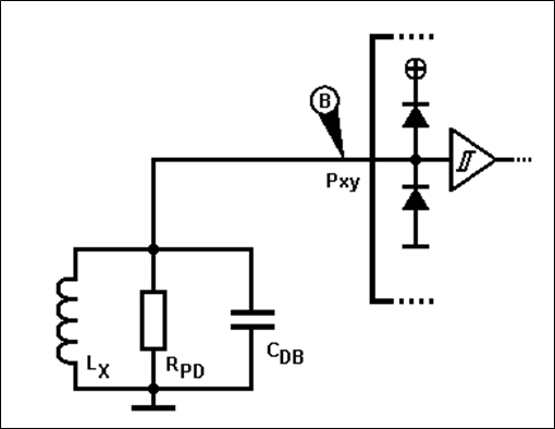
Figure 4. Principle switch circuit
R
PD
is a pull-down resistor and C
DB
a debounce capacitor. If the switch SW is open, a “0” is read from the port pin Pxy. When the switch is closed, the input changes to “1”.
From the physical aspect, consider that the switch is often placed at a distance from the MCU by trace, or circuit path. The longer the circuit path is, the higher will be its Inductance L
X
(and Capacitance C
X
).
An equivalent circuit diagram is shown in
Figure 5
.
Figure 5. Equivalent circuit of the principle switch circuit
By closing the switch SW at time t
0
, as shown in the voltage can be measured at point (A).
Figure 6. Signal rise after closing the switch at point (A)
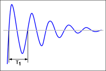
But, at the port pin Pxy on point (B), as shown
Figure 7
, voltage can be measured.
Figure 7. Signal rise after closing the switch at point (B)
By closing the switch SW, the circuit becomes a parallel oscillator with the wire-Inductance L
X
, the debounce Capacitance C
X
, and the Damping Resistance R
PD
of the pull-down resistor, as shown in
Figure 8
(it is assumed that it is an ideal power supply, with no internal resistance).
Figure 8. Equivalent circuit during closed switch
R
PD
is often chosen high (> 50 kΩ), and so its damping effect is weak.
This (weakly) attenuated oscillator causes voltage overshoots on the port pin (point (B)), as shown in red in .
Figure 9. Signal overshoots on port pin after closing the switch
These overshoots may cause an internal latch-up on the port pin, as the internal clamping diode connected to internal power supply becomes conductive. Similar is the effect, if the switch SW is opened. In this case, there are under shoots on the port pin.
The frequency of the oscillation can be calculated by following equation:
The inductance L
X
is an unknown value and depends on the PCB, its routing, and the trace length.
Solution A:
One solution is to decrease the capacitance of the debounce capacitor. This increases the oscillation frequency and the over-all energy of the overshoot is lesser.
Figure 10. Bounce signal on the pin with a large capacitance
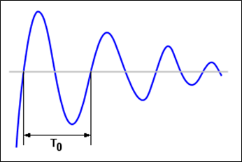
Figure 11. Bounce signal on the pin with a small capacitance
This solution has two disadvantages: the debounce effect decreases and there is no guarantee that the latch-up condition is eliminated.
Solution B: (recommended)
A recommended solution is to use a series resistor (R
S
) at the port pin as shown in
Figure 12
.
Figure 12. Recommended switch circuit with series resistor
The series resistor R
S
reduces the amplitude of the oscillation and decreases the voltage offset at first. If resistance of Rs is too high, the input voltage (Vp) at port pin will be below the logic high threshold required by the logic family such as CMOS/TTL (for example, CMOS/TTL/Automotive level).
Figure 13. Reduction of the signal bouncing on the pin due to the series resistor
5-V tolerant input pins
The PSoC™ 4 HV PA device input pins are not 5-V tolerant. If the application uses an I2C bus system with 5 V, an external level shifter is required to avoid latch-up effect on the MCU pin.
Reset behavior of IO port pins
During and after the POR, all GPIOs are in HIGH-Z analog state and the input buffers are disabled. During runtime, GPIOs can be configured by writing to the associated registers. The DAP connection can be disabled or reconfigured for general-purpose use only after the code execution starts.
Glitch filtering
The MCU provides the option of internal glitch filtering.
Glitch filter
The IO system can implement the glitch filter. In the Deep Sleep mode, either the internal low-speed oscillator (ILO) or the precision internal low-speed oscillator (PILO) clock can be selected as the clock source. (see
Table 3
). For more information, see I/O System in the
Architecture TRM
.
See
Latch-up consideration (Switch)
for the latch-up considerations regarding deployed external filters.
Figure 14. Port glitch filter and interrupt structure
Mode pin
A dedicated Mode pin is not required to enter the PSoC™ 4 HV PA into programming or normal run mode.
External interrupt input pins
In general, an external interrupt can be captured by edge detection on every general-purpose I/O (GPIO) port pin. See
Glitch filtering
on how to use glitch filtering.
lists the wakeup sources in the different power modes. For more details on the power modes, see System Resources Subsystem (SRSS), Device Power Modes in the corresponding
reference manual
.
Port pin function | External interrupt/wakeup in power mode | ||
|---|---|---|---|
Active | Sleep | DeepSleep | |
GPIO | ✓ | ✓ | ✓ |
LIN 2 | ✓ | ✓ | ✓ |
SCB | ✓ | ✓ | ✓ |
Flash programming connection
The Flash programming can be done with the SWD connection. Hence, no mode pins are available to switch the device into a programming mode after POR. See
Debug interface
for information on the debug connections.
Debug interface
The serial wire debug (SWD) interface is used as the communication protocol between the external device and PSoC 4 HV PA. There are several options to connect the debug system to the MCU depending on the debug requirements and the tool chain support. The following are the debug connectors:
Legacy 20-pin Insulation Displacement Contact (IDC) Connector
10-pin Arm® Cortex® Debug Connector
20-pin Arm® Cortex® Debug Connector
The JTAG and SWD signals are shared among these connections. The differences of
Figure 15
and
Figure 16
are indicated by marking the SWD protocol signals in blue. Note that PSoC™ 4 HV PA only supports SWD interface.
Legacy 20-pin IDC connector
The legacy JTAG/SWD interfaces are used for Flash programming and debugging. The SWD signals can be shared.
Note: The interface terminates in a 20-way, 2.54 mm pitch IDC-connector (for example, Hirose HIF3FC-20PA-2.54DSA).
Figure 15. Legacy 20-pin IDC connector
10-pin
Arm® Cortex®
debug connector
To use the SWD debug interface, a 10-pin MIPI connector is defined with the minimum number of signals required for debugging. The JTAG interface signals are replaced by the bidirectional data signal (SWDIO) and the clock signal (SWCLK). The freed up TDO signal can be reused as a system trace data output serial wire output (SWO).
Note:
For the SWD debugging, a 10-way connector with 1.27 mm pitch is applied (for example, Samtech FTSH-105-01-L-DV-K).
Position 7 (KEY) has no pin and serves only as a key to properly orient the connector.
Figure 16. 10-pin Arm® Cortex® debug connector
20-pin
Arm® Cortex®
debug connector
To use the SWD debug interface, a 20-pin MIPI connector is defined with the minimum number of signals required for debugging.
Note:
PSoC™ 4 HV PA only supports SWD.
As a connector, a 20-way 1.27 mm pitch IDC-connector is applied (for example Samtech FTSH-110-01-L-DV-K).
Position 7 (KEY) has no pin and serves only as a key to properly orient the connector.
Figure 17. 20-pin Arm® Cortex® debug connector
Termination resistors
If the debug connection is a long trace, recommend to optionally connect the termination resistors. Also, the external termination resistors are not required for this MCU, after POR default SWD Interface (I/F) is enabled in the boot ROM.
SWD mode | Signal | Required termination resistor | MCU implementation |
|---|---|---|---|
SWCLK | Clock into debug core | 1 k – 100 kΩ pull-down resistor to GND | Pull-down resistor |
SWO | Trace data output | _ | _ |
SWDIO | SWD Data In / Out | 1 k – 100 kΩ pull-up resistor to VDDD | Pull-up resistor |
GND | Connection to system ground | _ | _ |
and
Figure 19
show how to connect the debug connector to the MCU. In general, it is recommended to place a series resistor (20Ω) closer to the connector to avoid reflections and ringing of the debug clock signal. Otherwise, with strong oscillations near the input voltage threshold, the debug I/F can interpret wrong data. Note that due to the internal termination resistor, a possible voltage divider in the debug clock signal might be required.
Figure 18. Debug connection to the MCU with 20-pin IDC and Arm® Cortex® debug connector
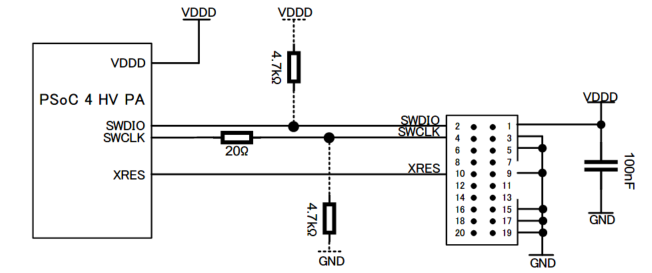
Figure 19. SWD debug connection to the MCU with 10-pin Arm® Cortex® debug connector
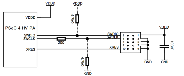
Note: PSoC™ 4 HV PA does not support external In-Circuit Emulator (ICE) power supply. Supply power to the VBAT pin with an external adapter (12 V).
Clock output function
You might need to cross-check the MCU internal clock signals for evaluation purposes. You can cross-check with the following options:
EXT_CLK port pin
Internal clocks can be routed through a divider to the alternate function port pin EXT_CLK as a clock output function. The EXT_CLK pin is a bi-directional pin, therefore, it can also be used as an external clock source. See section
Clock sources (Internal and external)
for more information on this pin.
As the MCU clock output functionality drives fast digital signal, this signal must be routed far away from the analog input and the analog voltage reference signals.
Alternate output function pin
The system clocks can be implicitly observed by using a PWM signal coming from a TCPWM output channel for instance. Note that each TCPWM channel input clock is derived by a dedicated clock divider of the peripheral clock. See Clocking System in the
reference manual
for more details on the clock tree.
Layout and electromagnetic compatibility
General
To avoid ESD problems and noise emission of the system, consider some rules for the layout design.
The most critical point is the VCCD pin, as this is the connection to the internal supply for the MCU core. Place the required decoupling capacitors as close as possible to this pin. Usually a bigger buffer or Decoupling capacitor of μF range is added to the dedicated power domain to Decoupling the period until the capacitors are recharged again. Otherwise, Decoupling capacitors and finally the system will fall below the power supply operating range.
If possible, place all decoupling capacitors on the same mounting side as the MCU. Alternatively, you could place the Decoupling capacitors on the bottom layer below the paired power supply pins (for example, VDD/VSS pair).
The analog supply should be decoupled from the digital supply. A common ground should be as far as possible from the MCU if you use the separated ground. In the hardware design, make sure that no latch up effect between the digital and analog supply or between analog and digital ground can occur. Therefore, the impedance between the different VSS pins, between analog ground and analog reference input need to be as low as possible.
Power supply pins
Ground and power supply
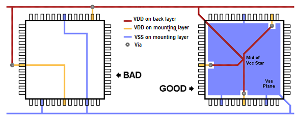
In general, the corresponding VDD and VSS lines should not be routed in chains, but in star shape.
shows an example of a bad and a good power line routing.
Figure 20. Generic example of bad vs. good power line routing
For a multi-layer PCB, the VDD and VSS should be routed as a plane in the inner layers of PCB. Considering a layer stack with several power supply planes, these planes should not overlap to avoid noise coupling.
Here are some recommendations for good EMC behavior:
Use a multi-layer PCB
Use power supply planes (ground and power) in the inner-layer of PCB layer stack.
Place one or two decoupling capacitors close to each corresponding supply pin pair to reduce the possible radiation.
Use capacitor groups to match the frequency behavior of power supply decoupling. The decoupling capacitors can have values between 1 nF and 10 μF.
Make sure that only one common star point connects analog and digital ground planes to each other. To have less noise on the analog part, the star point should be placed as far as possible from the MCU and as close as possible to the voltage regulator capacitor to the Electronic Control Unit (ECU) connector.
Make sure that the digital and analog planes do not overlap and interfere. Furthermore, there should be no signal plane between these planes.
Shield the analog input signals by the analog ground as much as possible.
Avoid ground loops.
Make sure that the supply traces with a layer changeover have at least two vias.
shows an example of a bad PCB Layer Stack, as there might be crosstalk between different power supply planes. However,
Figure 22
is an example of well-designed PCB layer stack in which the analog and digital supply planes are separated in the common layer. Thus, the EMC behavior of the board is already improved.
Figure 21. Example of a bad PCB layer stack
Figure 22. Example of a good PCB layer stack
Power supply decoupling
Placement
In general, the Decoupling capacitors should be placed as close as possible to MCU. When a small ceramic capacitor is used together with a large electrolytic capacitor for decoupling, place the ceramic capacitor closer to the MCU power supply rail than the electrolytic capacitor.
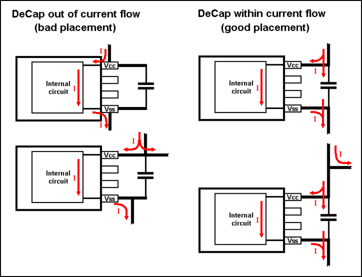
Decoupling capacitors for power supply must be placed within the current flow. If not, they are useless as their function becomes less efficient as shown in
Figure 23
. As the description is valid for generic use, as shown in
Figure 23
to
Figure 25
, the generic naming convention for power supply pins is VCC and for ground pins is VSS.
Figure 23. Power supply decoupling capacitor placement
Usually the noise current should flow through the soldering pad of decoupling capacitor C
B
.
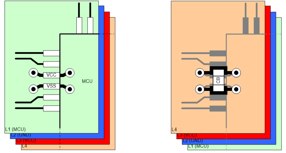
Figure 25
shows the recommended routing and placement on the boards.
Figure 24. Recommended power supply decoupling on boards
shows an alternate routing and placement, though not recommended. Note that the capacitor is placed on the opposite PCB side like the MCU. This solution is best suited for high-density board assembly.
Figure 25. Alternate power supply decoupling on boards
I /O domains
The dimensioning of the Decoupling capacitors for the I/O domain is application specific. Consider the following points while dimensioning:
What is the switching behavior (periodic or random) of the output stages and what is the transition requirement?
How many outputs have the same transition at the same time during the running operation or after any wake up or reset?
How big is the capacitive load at one output pin?
Which driver strength configuration is selected?
Is there any DC current caused by resistors, which might be also buffered by big Decoupling capacitor?
It is strongly recommended to make either a Power Distribution Network (PDN) analysis with an IBIS model or test on the PCB. A simplified consideration about the decoupling is provided in
SRAM Board Design Guidelines
.
Component placement
Place the analog components such that the ground connection is on a common partition area. Do the same for digital components. Place the analog voltage reference regulator over the analog plane and the digital voltage regulator accordingly over the digital plane.
Make sure that the components with a common power supply are located as centrally as possible to each other.
Place the MCU and other mixed signal components accordingly on the PCB so that it acts as a bridge between the analog and digital partitions.
Signal routing
Make sure that the digital power and signal traces are routed over the digital ground planes and analog power and signal traces are routed over the analog ground plane.
To isolate analog signals traces, make sure that the areas around the traces are filled with copper, which are connected to analog ground plane. The same recommendation is also valid for areas with digital signal traces.
Do not route traces near to or parallel to other noisy and sensitive traces.
Keep the trace lengths as short as possible.
Furthermore, when designing an application, study the following areas closely to improve the EMC performance:
Noisy signals, for example, signals with fast rise/fall times
Sensitive and high-impedance signals
Signals that capture events, such as interrupts and strobe signals
Thermal considerations
Once an indication of the MCU total power requirement is known, it is very important to understand if the system design can properly dissipate this power into the ambient air efficiently enough to require no further action, or if significant heat sinking and PCB design choices might be required. Under certain conditions, MCUs may dissipate more than 0.5 W of power including the core, peripheral, and I/O currents. With a lot of power in a device, necessary steps are required to prevent overheating. Before a design is finalized, a complete thermal review should be done. Items such as the amount of airflow through the system, nearby heat sources, and PCB construction should be reviewed.
Calculation of junction temperature
T
J
: Junction Temperature
T
A
: Ambient Temperature
Θ
JA
: Thermal Resistance from Junction to Ambient
P
D
: Power Dissipation
The examples given below are the first steps to determine whether the preliminary design objectives can be met by the above equation.
For a first order approximation, first check the datasheet for the thermal resistance from junction to ambient (θ
JA
) for the target device package.
θ
JA
is expressed in units of °C/watt. For example, the θ
JA
for an QFN 32-pin is 14 °C/watt.
The maximum temperature difference between the device junction and the ambient air surrounding the device is θ
JA
times the maximum power, or as in the first case above 14°C/watt x 1.0 watt = 14 °C. The specified maximum operating junction temperature of the device is 150°C, so the maximum allowable ambient air temperature is 150 – 14 = 136 °C.
Each device datasheet includes the package thermal resistance and maximum permissible power. This allows you to quickly see the amount of power that can practically be consumed by a device in each package. The datasheet might include the recommended minimal PCB construction. So, for instance a four-layer PCB has better power dissipation characteristic than a two-layer PCB, because inner plane layers help to dissipate the heat.
Note: The datasheet specifications for θJA are typical value. The ambient air temperature should be lesser than the allowable maximum for the product design.
For more details, see the
application notes
.
Summary
The application note described the procedure to set up a hardware environment for PSoC™ 4 HV PA family. In addition, the application note also provided hints to handle different uses cases at MCU pins and to make a proper PCB layout design.
Abbreviations
Abbreviation | Description |
|---|---|
ALT | Alternate |
BOD | Brown-out-Detection |
BOM | Bill of material |
DS | Data sheet |
DUT | Device under test |
ECU | Electronic Control Unit |
ESD | Electro Static Discharge |
ETM | Embedded Trace Macrocell |
Ext | External |
GND | Electrical ground |
GPIO | General Purpose I/O |
HVD | High-Voltage-Detection |
IC | Integrated Circuit |
I/F | Interface |
Int | Internal |
IO | Input, Output |
JTAG | Joint Test Action Group is the common name for the IEEE 1149.1 Standard Test Access Port, Boundary-Scan Architecture, and interface for debug tools for on-chip debug inside the target MCU |
LVD | Low-Voltage-Detection |
MCU | Microcontroller, Microcontroller Unit |
PDN | Power Distribution Network |
PHY | PHYsical layer. Electrical component for data coding and decoding between pure digital and modulated channel |
S/s | Samples per second |
SCB | Serial Communication Block |
NC | Not connected |
OVD | Overvoltage Detection |
PCB | Printed Circuit Board |
POR | Power-On-Reset |
PWM | Pulse Width Modulation |
Rd | Damping resistor |
Rf | Feedback resistor |
STP | Shielded Twisted-Pair |
SWD | Serial Wire Debug |
TCPWM | Timer, Counter and PWM |
TRM | Technical Reference Manual |
VCC | Generic naming convention for power supply pin |
VSS | Generic naming convention for ground pin |
WDT | Watchdog Timer |
References
Application
notes
AN230264
- Getting Started with PSoC™ 4 HV PA Family
AN230370
- How to use Precision Analog Channel Subsystem in PSoC™ 4 HV PA Family
AN72845
- Design Guidelines for QFN Packaged Devices
AN80994
- Design Considerations for Electrical Fast Transient (EFT) Immunity
AN57821
- PSoC™ 3, PSoC™ 4, and PSoC™ 5LP Mixed Signal Circuit Board Layout Considerations
Arm
Developer
ARM_Link_01
- CoreSight Components Technical Reference Manual (Cortex debug connector detailed specification in appendix C)
Datasheet
PSoC™ 4 HV Precision Analog Datasheet
Reference Manuals
PSoC™ 4 HV PA Architecture Reference Manual (RM)
PSoC™ 4 HV PA Registers Reference Manual (RM)
Contact Technical Support to obtain PSoC™ 4 HV PA family series datasheets and Technical Reference Manuals.
Revision history
Document version | Date of release | Description of changes |
|---|---|---|
** | 2020-12-04 | Initial release |
*A | 2021-02-23 | Added reference to AN230370 Updated Port input/unused pins Added Table 4 |
*B | 2023-04-19 | Template update; no content updated. |
1
ECO is not available in PSoC™ 4 HV PA device. It will be available in upcoming products.