AN230370 Precision analog channel subsystem in PSoC™ 4 HV PA family
About this document
Scope and purpose
This application note introduces you to the precision analog channel subsystem (PACSS) of PSoC™ 4 HV precision analog (PA) family MCUs. This application note also guides you to develop hardware and firmware design for battery monitoring application.
Intended audience
This document is intended for hardware and firmware design engineers.
Introduction
This application note provides an overview of the precision analog channel subsystem (PACSS) with the CY8C41xxLCE-HV4xx series from the PSoC™ 4 high-voltage (HV) precision analog (PA) family. PSoC™ 4 HV PA is a fully integrated programmable embedded system for battery monitoring and management. The system features an Arm® Cortex® M0+ processor and programmable and reconfigurable analog and digital blocks. To get a better understanding of the PACSS functionality and terminology used in this application note, it is a good idea to read "Section 21. Precision analog channel subsystem" of the
architecture reference manual (RM)
.
Precision analog channel subsystem overview
The PSoC™ 4 HV PA precision analog channel subsystem (PACSS) is a high-performance data acquisition subsystem consisting of two physical analog channels and four physical digital channels. The PACSS contains of the following blocks:
Analog delta-sigma modulator (DSM) system
Two analog channels
Channel multiplexer
Digital data system
Four digital channels (with/without FIR filter)
Data storage
Automatic gain control
Gain multiplexer
I/O components
Input multiplexer
Two high-voltage (HV) input dividers
On-die temperature sensor
External temperature sensor
shows the detailed block diagram of the PACSS measurement and acquisition system.
The analog DSM system is composed of the input multiplexer, programmable gain amplifier (PGA), anti-alias filter (AAF), diagnostic multiplexer, buffer, and a delta-sigma modulator. The digital data system is comprised of the scaler, decimator, FIR-type digital filter, accumulator, comparator, and offset and gain calibrations.
Also included in this subsystem are the auto gain correction (AGC) circuit and a temperature sensor with diagnostic capability. Each digital channel can quickly switch between input sources to create a "virtual" ADC that shares one of the analog channels, by using the digital data system. This “virtual” ADC channel can be used for diagnostic purposes.
The sequencer is used to generate control signals for performing all the functions of the channel.
Figure 1. PACSS measurement and acquisition system
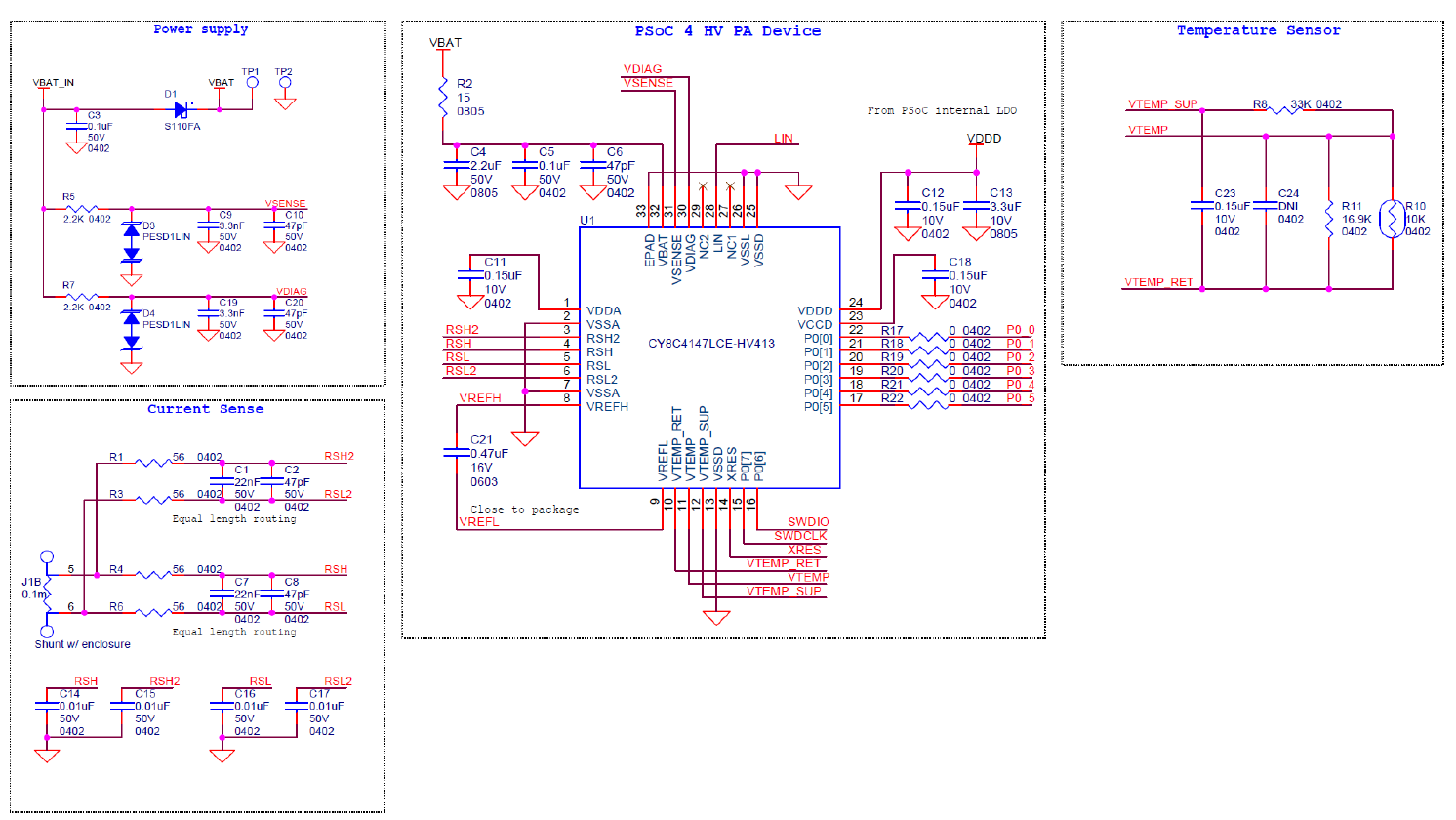
Schematic and layout example
shows general schematic of external circuit for the PACSS system of the PSoC™ 4 HV PA MCU. See
AN230265 - Hardware design guide
for more information of power block.
Figure 2. General schematic of external circuit for PACSS system
Current sensor line
Schematic example
The current sensor line uses the RSH/RSL and RSH2/RSL2 terminals of the PSoC™ 4 HV PA MCU (See
Figure 3
). The RSH/RSL terminals are for the main line, and the RSH2/RSL2 terminals are for diagnostics. In the circuit example below, the sense output of one shunt resistor is routed to both RSH/RSL and RSH2/RSL2 terminals.
The external resistor and capacitor are optional low-pass filter components to attenuate any external noise for your application.
shows an example of external components.
Figure 3. Schematic example of current sensor line
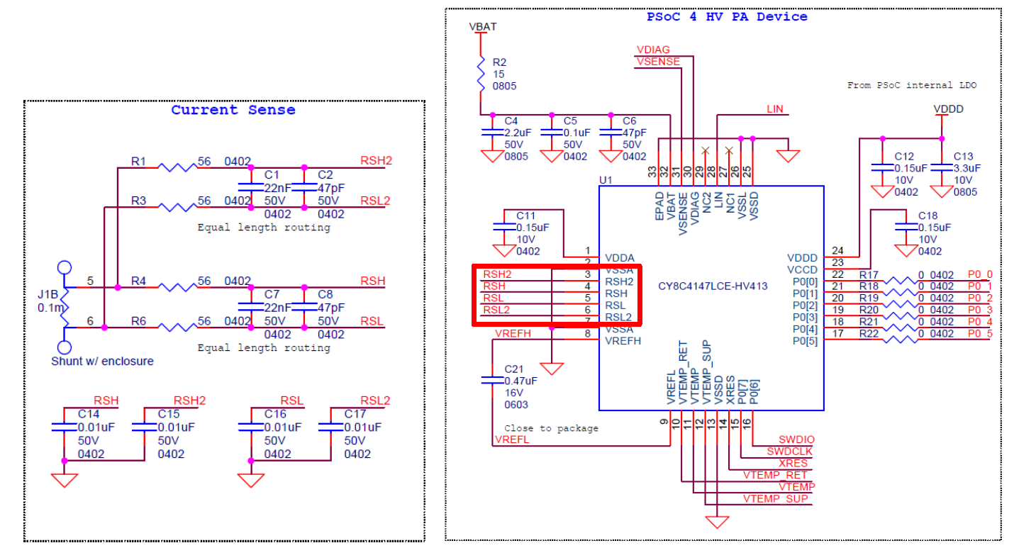
Symbol | Overview | Parameter | ||
|---|---|---|---|---|
Value 1 | Value 2 | Remark | ||
R1, R3, R4, R6 | Resistor for external noise filter | 56 Ω ± 1% | > 1/10 W | |
C1, C7 | Capacitor for external noise filter | 22 nF X7R | > 50 V | |
C2, C8 | Capacitor for external noise filter | 47 pF C0G | > 50 V | |
C14, C15, C16, C17 | Capacitor for external noise filter | 0.01 μF X7R | > 50 V | |
Note: Max resistor value for current path (R1/R3/R4/R6): 500ohm.
Layout example
shows an example of current sensor line layout. Note that RSH2/RSL2 components are placed on bottom layer which are same position as RSH/RSL. This figure only shows top layer.
Figure 4. Layout example of current sensor line
Follow these guidelines for the design of the current sensor line circuit on the PSoC™ 4 HV PA MCU:
Match the length of each pair of RSHx and RSLx traces by routing on top or bottom layers of the PCB
Keep the width of RSHx/RSLx traces as the same as the IC Pad width
Do not use through-hole vias on the RSH/RSL trace if possible
Connect shunt resistor tracks from the inner edges of its solder pad to the IC as a differential pair
Keep the distance between RSHx and RSLx traces as the same as the IC terminal pitch if possible
Guard the entire pattern with GND
Place the GND layer under the sensor lines
Voltage sensor line
Schematic example
The voltage sense line uses the VSENSE and VDIAG terminals of the PSoC™ 4 HV PA MCU (See
Figure 5
). The VSENSE terminal is for the main line, while the VDIAG terminal is for diagnostic. In the circuit example below, the battery voltage input (VBAT) is divided into two and input to each terminal.
VSENSE and VDIAG inputs are normally connected directly to the battery with a series 2.2-kΩ resistor to measure the battery voltage; the capacitors are for low-pass filtering. The external transient voltage suppressors (TVS) diodes are to protect ESD noise. The TVS diodes are optional components.
shows an example of external components.
Figure 5. Schematic example of voltage sensor line
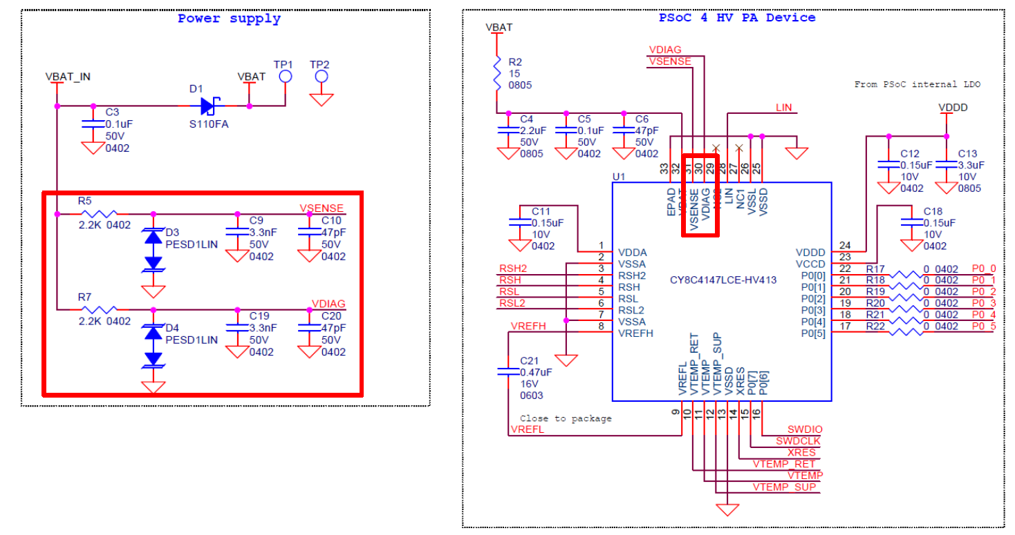
Symbol | Overview | Parameter | ||
|---|---|---|---|---|
Value 1 | Value 2 | Remark | ||
R5, R7 | Resistor for external noise filter | 2.2 kΩ ± 1% | > 1/10 W | |
D3, D4 | Transient voltage suppressor (TVS) | Bidirectional | Clamping voltage 44 V | Optional |
C9, C19 | Capacitor for external noise filter | 3.3 nF X7R | > 50 V | |
C10, C20 | Capacitor for external noise filter | 47 pF C0G | > 50 V | |
Note: Resistor values for voltage path (R5/R7): any deviation from nominal 2.2 kilohm needs to be associated with a reduction in accuracy.
Layout example
shows an example of the voltage sensor line layout.
Figure 6. Layout example of voltage sensor line
Follow these guidelines for the design of voltage sensor line circuit on the PSoC™ 4 HV PA MCU:
Length match the VSENSE and VDIAG traces as close as possible
Wire the VSENSE and VDIAG sensor lines from each VBAT point
Keep the trace width in the range of "0.127 mm" to the "IC terminal width"
Guard the entire pattern with GND
Place the GND layer under the sensor line
Temperature sensor line
Schematic example
The temperature sensor line uses the VTEMP_SUP, VTEMP, and VTEMP_RET terminals of the PSoC™ 4 HV PA MCU (See
Figure 7
). VTEMP_SUP terminal is the power supply for the external temperature sensor, VTEMP is the temperature voltage input from the external sensor, and VTEMP_RET is the ground signal. In the circuit example below, the capacitors are added for decoupling the temperature sensor line.
The external voltage divider is selected to optimize temperature accuracy and will typically be comprised of a 33-kΩ and 16.9-kΩ fixed resistors (R) and a 10-kΩ nominal NTC thermistor RT (nominal NTC resistance is typically specified at 25°C).
shows an example of external components.
Figure 7. Schematic example of temperature sensor line
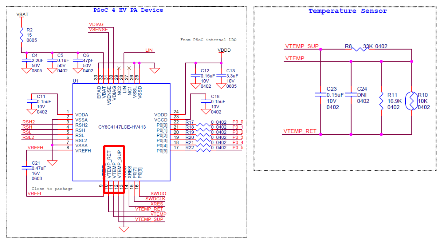
Symbol | Overview | Parameter | ||
|---|---|---|---|---|
Value 1 | Value 2 | Remark | ||
R8 | Resistor for voltage divider | 33 kΩ ± 1% | > 1/10 W | |
R10 | Thermistor | 10 kΩ ± 1% | > 1/8 W | |
R11 | Resistor for voltage divider | 16.9 kΩ ± 1% | > 1/10 W | |
C23 | Capacitor for external noise filter | 0.15 μF X7R | > 10 V | |
Layout example
shows an example of temperature sensor line layout.
Figure 8. Layout example of temperature sensor line
Follow these guidelines for the design of temperature sensor line circuit on the PSoC™ 4 HV PA MCU:
Place the thermistor (R10) as close to hot spot as possible
Keep the VTEMP_SUP, VTEMP, and VTEMP_RET at the same length as possible
Place the filter capacitor (C24) near the VTEMP and VTEMP_RET terminal
Keep the trace width in the range of "0.127 mm" to "IC terminal width"
Guard the entire pattern with GND
Place the GND layer under the sensor line
Battery minus and chassis GND connection
The PSoC™ 4 HV PA MCU can connect a battery minus and chassis GND to each current sensor line (RSH/RSL) and silicon GND (VSSA).
Figure 9
shows the general application block diagram for the intelligent battery system.
This example connects RSH and VSSA to chassis GND and connects RSL to battery minus. In this case, PACSS output will be #1 results in
Table 4
. The output data includes the consumed current of the PSoC™ 4 HV PA board as shown in green (when VSSA connects chassis GND). The polarity will be positive when discharging the battery and negative in charging the battery (When RSH is connected to chassis GND).
User can select the suitable GND connection for your application from
Table 4
.
Figure 9. General application block diagram for intelligent battery system
GND connection | Block diagram | PACSS output | ||
|---|---|---|---|---|
Polarity | Data | |||
1 | RSL - Battery minus RSH - Chassis GND VSSA - Chassis GND | Discharge: Plus Charge: Minus | Includes the consumed current of the PSoC™ 4 HV PA board | |
2 | VSSA - Battery minus RSL - Battery minus RSH - Chassis GND | Discharge: Plus Charge: Minus | Does not include the consumed current of the PSoC™ 4 HV PA board | |
3 | VSSA - Battery minus RSH - Battery minus RSL - Chassis GND | Discharge: Minus Charge: Plus | Does not include the consumed current of the PSoC™ 4 HV PA board | |
4 | RSH - Battery minus RSL - Chassis GND VSSA - Chassis GND | Discharge: Minus Charge: Plus | Includes the consumed current of PSoC™ 4 HV PA board | |
PACSS firmware configuration
Infineon provides the sample driver library (SDL) including startup code as sample firmware. The SDL provides a simple interface to access various peripherals and is used for system validation, hardware bring-up, benchmarks, feasibility studies, and demos. The SDL cannot be used for production purposes because it is not qualified with any automotive standards. The SDL integrates device header files, startup code, and peripheral drivers. The SDL contains a set of firmware drivers that provide APIs for accessing device-specific resources. See
AN230264 - Getting started with PSoC™ 4 HV PA family
for detailed SDL information.
The following sections explain the details of the application programming interface (API) and code examples for PACSS.
Attention: PACSS firmware configuration is created based on SDL version 3.0.0.
Peripheral drivers
Peripheral drivers are a set of firmware drivers that provide APIs for accessing the hardware. These APIs perform initialization and control activities of each peripheral.
Table 5 lists and describes the interface to each PACSS function. The peripheral drivers of PACSS are located in SDL path of:
C:/<user path>\ PSoC_Sample_Driver_Library_x.x.x\psoc4hvXXXk\src\drivers\adc\rev_b
Note: The PACSS has many registers to configure it. Table 5 is simplifying to only expose controls the customer should be using. See "low_level" and "config" folders in above path for more detailed functions.
See
API details
for more information.
Function | Description |
|---|---|
cy_adc.c | |
Cy_Adc_StartConversion() | Trigger a conversion on the enabled primary channels |
Cy_Adc_StartSecondaryConversion() | Trigger a secondary conversion on the enabled secondary channels |
Cy_Adc_GetResult() | Read the value in the result register of the specified channel |
Cy_Adc_GetAccumulatorResult() | Read the value in the accumulated result register of the specified channel |
Cy_Adc_ResetAccumulator() | Reset the accumulator to zero |
Cy_Adc_SetAccumulatorThreshold() | Set the accumulator Threshold |
Cy_Adc_SetGroundReference() | Set the ground connection for the high-voltage divider |
Cy_Adc_EnableSequencer() | Enable the ADC sequencer and AREF |
Cy_Adc_DisableSequencer() | Disable the ADC sequencer |
Cy_Adc_EnableReference() | Configure and enable the high-precision band gap reference (HPBGR) |
Cy_Adc_DisableReference() | Disable the high-precision band gap reference (HPBGR) |
Cy_Adc_GetInterrupt() | Get the specified digital channel's interrupt status |
Cy_Adc_GetInterruptMasked() | Get the DCHAN interrupt status masked by the enabled interrupts |
Cy_Adc_SetInterruptMask() | Enable the specified interrupt type for the specified channel |
Cy_Adc_ClearInterrupt() | Clear the specified interrupt |
Cy_Adc_GetInterruptCause() | Get the interrupt cause |
Cy_Adc_SetGainCorrection() | Set the gain correction factor for the specified DCHAN |
Cy_Adc_SetOffsetCorrection() | Set the offset correction factor for the specified DCHAN |
Cy_Adc_SetAGCGainCorrection() | Set the gain correction factor for the specified AGC gain level |
Cy_Adc_SetAgcOffsetCorrection() | Set the offset correction factor for the specified AGC gain level |
Cy_Adc_SetVrefLow() | Set the selection of the low reference of the DCHAN |
Cy_Adc_SetVrefHigh() | Set the selection of the high reference of the DCHAN |
cy_adc_init_achan.c | |
Cy_Adc_EnableAchan() | Enable the analog channel |
Cy_Adc_DisableAchan() | Disable the analog channel |
Cy_Adc_InitAchan() | Configure the analog channel |
ConfigureBuffer() | Configure the analog channel buffer |
ConfigurePga() | Configure the analog channel programmable gain array |
ConfigureReference() | Configure the analog channel reference |
ConfigureModulator() | Configure the analog channel modulator |
ConfigureTrigger() | Configure the analog channel primary/secondary trigger |
cy_adc_init_agc.c | |
Cy_Adc_EnableAgc() | Enable automatic gain correction (AGC) |
Cy_Adc_DisableAgc() | Disable automatic gain correction (AGC) |
Cy_Adc_InitAgc() | Configure automatic gain correction (AGC) |
ConfigureGainLevel() | Configure the gain level in memory, given the input configuration |
cy_adc_init_channel_chopping.c | |
Cy_Adc_InitAchanChannelChopping() | Configure the selected analog channel to perform channel chopping. |
cy_adc_init_dchan.c | |
Cy_Adc_EnableDchan() | Enable the digital channel |
Cy_Adc_DisableDchan() | Disable the digital channel |
Cy_Adc_InitDchan() | Configure the digital channel |
Cy_Adc_ConfigureGainLevel() | Configure the digital channel gain level settings |
ConfigureFIRFilter() | Configure the digital channel FIR filter coefficients |
Cy_Adc_ConfigureAafMode() | Configure the anti-alias filter |
cy_adc_init_temperature.c | |
Cy_Adc_EnableTemperature() | Enable the temperature sensor |
Cy_Adc_DisableTemperature() | Disable the temperature sensor |
Cy_Adc_InitTemperature() | Configure the temperature sensor |
Code example
Dual convert design (current/voltage)��
This example uses "current" channel (ACHAN0) that continuously measures the voltage across the RSH/RSL shunt resistor, and a second channel (ACHAN1) measures the voltage across the HV voltage divider with 16x attenuation. The current and voltage channel use the FIR filter. The results display in millivolts over the UART connection. The code example is located in SDL path of:
C:/<user path>
PSoC_Sample_Driver_Library_x.x.x\psoc4hvXXXk\src\examples\adc\dual
Each block configuration:
ACHAN 0/DCHAN0 configuration - current sensor
Continuous sampling mode
Primary channel
Stage 1 decimation filter: Sync 3, DR = 64
Stage 2 decimation filter: Sync 1, DR2 = 6
Sampling shunt resistor across RSL and RSH
Zero channel select delay (since this DCHAN has a dedicated ACHAN)
15-tap FIR filter
Accumulate four samples
ACHAN 1/DCHAN1 configuration - voltage sensor
Continuous sampling mode
Primary channel
Stage 1 decimation filter: Sync 3, DR = 64
Stage 2 decimation filter: Sync 2, DR2 = 6
Sampling the high-voltage divider between VSENSE and GND
Zero channel select delay (since this DCHAN has a dedicated ACHAN)
15-tap FIR filter
Unity gain
shows the PACSS sequencer timing for dual convert design.
Figure 10. PACSS sequencer timing of dual convert design
Note: The ADC is sampling much faster than the UART output so not all sampled results will be transmitted. This applies to all of the examples.
shows the flow chart for dual convert design, and
Code Listing 1
shows the code example of main function.
Note: User should compare the code example with the flowchart, and learn how to use the PACSS functions. You cannot copy/paste the code and expect it to work. This applies to all code examples provided in this document.
Figure 11. Flowchart of dual convert design
Code Listing 1 Main function of dual convert design
001 int main(void)
002 {
003 cy_en_adc_error_t error = CY_ADC_ERROR;
004 int32_t currentChannelResult = 0;
005 int32_t voltageChannelResult = 0;
006 float32_t millivoltsAcrossShunt = 0.0;
007 float32_t batteryVoltage = 0.0;
008
009 SystemInit();
010
011 /* Enable DCHAN0 Interrrupt */
012 Cy_SysInt_EnableIRQ(CY_PACSS_ADC_DCHAN0_IRQN);
013 Cy_SysInt_SetVector(CY_PACSS_ADC_DCHAN0_IRQN, Adc_Dchan0_IntrISR);
014 Cy_SysInt_ClearPendingIRQ(CY_PACSS_ADC_DCHAN0_IRQN);
015 Cy_Adc_SetInterruptMask(PACSS_DCHAN0, CY_ADC_DCHAN_INTERRUPT_DATA_VAL);
016
017 /* Enable DCHAN1 Interrrupt */
018 Cy_SysInt_EnableIRQ(CY_PACSS_ADC_DCHAN1_IRQN);
019 Cy_SysInt_SetVector(CY_PACSS_ADC_DCHAN1_IRQN, Adc_Dchan1_IntrISR);
020 Cy_SysInt_ClearPendingIRQ(CY_PACSS_ADC_DCHAN1_IRQN);
021 Cy_Adc_SetInterruptMask(PACSS_DCHAN1, CY_ADC_DCHAN_INTERRUPT_DATA_VAL);
022
023 /* Enable global interrupts. */
024 __enable_irq();
025
026 Example_UartInit();
027
028 /* Divide 24 MHz HF clock to get 3 MHz PACSS Clock */
029 Cy_SysClk_PeriphAssignDivider(CY_PACSS_ADC_PCLK, CY_SYSCLK_DIV_16_BIT,
030 PACSS_DSM_CLK_PERI_DIVIDER_NUM);
031 Cy_SysClk_PeriphSetDivider(CY_SYSCLK_DIV_16_BIT,
032 PACSS_DSM_CLK_PERI_DIVIDER_NUM,
033 CY_ADC_PERIPHERAL_CLOCK_DIVIDE_3 MHz);
034
035 /* Enable peripheral divider */
036 Cy_SysClk_PeriphEnableDivider(CY_SYSCLK_DIV_16_BIT,
037 PACSS_DSM_CLK_PERI_DIVIDER_NUM);
038
039 /* Set the pump clock source to the IMO */
040 Cy_SysClk_SetSourcePumpClk(CY_SYSCLK_PUMP_SEL_IMO);
041
042 /* Enable the HV Divider on VSENSE */
043 Cy_Hvss_Rvid_EnableVS0();
044
045 /***************************************************************************
046 * Configure the PACSS
047 **************************************************************************/
048 Cy_Adc_EnableSequencer(PACSS_MMIO);
049 Cy_Adc_EnableReference(PACSS_MMIO);
050
051 /* Sequencer must be enabled 1000us before enabling any analog channels to
052 allow the reference currents to settle */
053 Cy_SysLib_DelayUs(CY_ADC_REFERENCE_DELAY_US);
054
055 /* ACHAN0 / DCHAN0 config */
056 error = Cy_Adc_InitAchan(PACSS_ACHAN0, &cy_stc_adc_achan0_config);
057 CY_ASSERT(CY_ADC_ERROR_NONE == error);
058 error = Cy_Adc_InitAchanChannelChopping(PACSS_ACHAN0,
059 &cy_stc_current_channel_chopping_config);
060 CY_ASSERT(CY_ADC_ERROR_NONE == error);
061 Cy_Adc_EnableAchan(PACSS_ACHAN0);
062 error = Cy_Adc_InitDchan(PACSS_DCHAN0, &cy_stc_adc_dchan0_config);
063 CY_ASSERT(CY_ADC_ERROR_NONE == error);
064 Cy_Adc_EnableDchan(PACSS_DCHAN0);
065
066 /* ACHAN1 / DCHAN1 config */
067 error = Cy_Adc_InitAchan(PACSS_ACHAN1, &cy_stc_adc_achan1_config);
068 CY_ASSERT(CY_ADC_ERROR_NONE == error);
069 error = Cy_Adc_InitAchanChannelChopping(PACSS_ACHAN1,
&cy_stc_voltage_channel_chopping_config);
070 CY_ASSERT(CY_ADC_ERROR_NONE == error);
071 Cy_Adc_EnableAchan(PACSS_ACHAN1);
072 error = Cy_Adc_InitDchan(PACSS_DCHAN1, &cy_stc_adc_dchan1_config);
073 CY_ASSERT(CY_ADC_ERROR_NONE == error);
074 Cy_Adc_EnableDchan(PACSS_DCHAN1);
075
076 /* Analog channel must be enabled for 3us before starting conversions */
077 Cy_SysLib_DelayUs(CY_ADC_ACHAN_DELAY_US);
078
079 /* AGC */
080 Cy_Adc_InitAgc(PACSS_MMIO, &cy_stc_adc_agc_config);
081 Cy_Adc_EnableAgc(PACSS_MMIO);
082
083 /* Calibrate the ADC channels */
084 Cy_Adc_CalibrateOffsetScalar(PACSS_DCHAN0);
085 Cy_Adc_CalibrateOffsetScalar(PACSS_DCHAN1);
086 Adc_Calibrate();
087
088 /* Start the conversion process */
089 Cy_Adc_StartConversion(PACSS_MMIO);
090
091 /* Opening UART Comment */
092 Example_UartPrintf("\r\nADC Dual Example\r\n");
093
094 /* Settle the FIR filters */
095 uint32_t voltageFilterSettle = 0;
096 uint32_t currentFilterSettle = 0;
097 while ((voltageFilterSettle < CY_ADC_FIR_NUM_TAPS) || (currentFilterSettle <
CY_ADC_FIR_NUM_TAPS))
098 {
099 if(g_voltageDataValid)
100 {
101 g_voltageDataValid = false;
102 voltageFilterSettle++;
103 }
104 if(g_currentDataValid)
105 {
106 g_currentDataValid = false;
107 currentFilterSettle++;
108 }
109 }
110
111 while (1)
112 {
113 if(g_currentDataValid)
114 {
115 g_currentDataValid = false;
116
117 Cy_Adc_GetResult(PACSS_DCHAN0, ¤tChannelResult);
118 millivoltsAcrossShunt = Cy_Adc_CountsToMillivolts(currentChannelResult,
119 CY_ADC_CURRENT_CHANNEL, CY_ADC_SAMPLE_RATE_8KSPS, CY_ADC_HBPGR_VOLTAGE);
120
121 Example_UartPrintf("Current (mV): %.2f\r\n", millivoltsAcrossShunt);
122 }
123
124 if(g_voltageDataValid)
125 {
126 g_voltageDataValid = false;
127
128 Cy_Adc_GetResult(PACSS_DCHAN1, &voltageChannelResult);
129 batteryVoltage = Cy_Adc_CountsToVolts(voltageChannelResult,
130 CY_ADC_VOLTAGE_CHANNEL,
131 CY_ADC_SAMPLE_RATE_8KSPS,
132 CY_ADC_HBPGR_VOLTAGE);
133
134 batteryVoltage = batteryVoltage * HVDIV_ATTENUATION;
135 Example_UartPrintf("Voltage (V): %.2f\r\n", batteryVoltage);
136 }
137 }
138 }
Triple convert design (current/voltage/temperature)
This example uses same configuration of current and voltage channels from the 'dual' example. Additionally, a third channel measures the external temperature at a 20-millisecond interval triggered by a PWM. The temperature measurement is a secondary measurement and it shares ACHAN1 with the battery voltage (VSENSE) measurement. The results display in millivolts over the UART connection. The code example is located in SDL path of:
C:/<user path>
PSoC_Sample_Driver_Library_x.x.x\psoc4hvXXXk\src\examples\adc\triple
Each block configuration:
ACHAN 0/DCHAN0 configuration - current sensor
Same as dual convert design
ACHAN 1/DCHAN1 configuration - voltage sensor
Same as dual convert design
ACHAN 1/DCHAN2 configuration - external temperature sensor
Single shot sampling mode
Secondary channel
Stage 1 decimation filter: Sync 3, DR = 64
Stage 2 decimation filter: Sync 2, DR2 = 1
Sampling the external temperature sensor (VTEMP and VTEMP_RET)
17 clock channel select delay to allow ADC to settle between input switching
VREFH of VDDA/3 and VREFL to VTEMP_RET to keep the measurement ratio-metric since the source for the thermistor circuit is VDDA
Unity gain
shows the PACSS sequencer timing for triple convert design.
Figure 12. PACSS sequencer timing of triple convert design
shows the flow chart for triple convert design, and
Code Listing 2
shows the code example of main function.
Figure 13. Flowchart of triple convert design
Code Listing 2 Main function of triple convert design
001	int main(void)
002	{
003	    cy_en_adc_error_t   error                       = CY_ADC_ERROR;
004	    int32_t             currentChannelResult        = 0;
005	    int32_t             voltageChannelResult        = 1;
006	    int32_t             temperatureChannelResult    = 1;
007	    float32_t           millivoltsAcrossShunt       = 0.0;
008	    float32_t           millivoltsTempSensor        = 0.0;
009	    float32_t           batteryVoltage              = 0.0;
010
011	    ~~~~~~ omitted (same as dual) ~~~~~~
012
013	    /* Enable DCHAN2 Interrrupt */
014	    Cy_SysInt_EnableIRQ(CY_PACSS_ADC_DCHAN2_IRQN);
015	    Cy_SysInt_SetVector(CY_PACSS_ADC_DCHAN2_IRQN, Adc_Dchan2_IntrISR);
016	    Cy_SysInt_ClearPendingIRQ(CY_PACSS_ADC_DCHAN2_IRQN);
017	    Cy_Adc_SetInterruptMask(PACSS_DCHAN2, CY_ADC_DCHAN_INTERRUPT_DATA_VAL);
018
019	    __enable_irq(); /* Enable global interrupts. */
020
021	    /* Initialize GPIOs for measuring temperature */
022	    External_TempSensorInit();
023
024	    ~~~~~~ omitted (same as dual) ~~~~~~
025
026	    /*--------------------------------*/
027	    /* Clock Configuration for TCPWM */
028	    /*--------------------------------*/
029
030	    /* Assign a programmable divider for TCPWM_CNT0 */
031	    Cy_SysClk_PeriphAssignDivider(PCLK_TCPWM_CLOCKSx_COUNTER,
032	                                  (cy_en_divider_types_t)CY_SYSCLK_DIV_16_BIT,
033	                                  TCPWM_CNT_CLK_PERI_DIVIDER_NUM);
034	    Cy_SysClk_PeriphSetDivider((cy_en_divider_types_t)CY_SYSCLK_DIV_16_BIT,
035	                               TCPWM_CNT_CLK_PERI_DIVIDER_NUM, TCPWM_CLOCK_16DIV);
036	    Cy_SysClk_PeriphEnableDivider((cy_en_divider_types_t)CY_SYSCLK_DIV_16_BIT,
037	                                  TCPWM_CNT_CLK_PERI_DIVIDER_NUM);
038
039	    /* Set the pump clock source to the IMO */
040	    Cy_SysClk_SetSourcePumpClk(CY_SYSCLK_PUMP_SEL_IMO);
041
042	    // Enable the HV Divider on VSENSE
043	    Cy_Hvss_Rvid_EnableVS0();
044
045	    /* Assign PWM compare match to ADC Trigger 0 */
046	    Cy_TrigMux_Connect(TRIG2_IN_TCPWM_TR_COMPARE_MATCH0, TRIG2_OUT_PACSS_TR_START0);
047
048	    /***************************************************************************
049	     * Configure the PACSS
050	     **************************************************************************/
051
052	    ~~~~~~ omitted (same as dual) ~~~~~~
053
054	    // Temperature Sensor
055	    Cy_Adc_EnableTemperature(PACSS_MMIO);
056
057	    ~~~~~~ omitted (same as dual) ~~~~~~
058
059	    error = Cy_Adc_InitDchan(PACSS_DCHAN2, &cy_stc_adc_dchan2_config);
060	    CY_ASSERT(CY_ADC_ERROR_NONE == error);
061	    Cy_Adc_EnableDchan(PACSS_DCHAN2);
062
063	    ~~~~~~ omitted (same as dual) ~~~~~~
064
065	    Cy_Adc_CalibrateOffsetScalar(PACSS_DCHAN2);
066
067	    ~~~~~~ omitted (same as dual) ~~~~~~
068
069	    /* Initialize TCPWM_CNTx_COUNTER in PWM Mode & Enable */
070	    Cy_Tcpwm_DisableCounter(TCPWM_CNTx_COUNTER);
071	    Cy_Tcpwm_Pwm_Init(TCPWM_CNTx_COUNTER, &cy_stc_pwm_config);
072	    Cy_Tcpwm_EnableCounter(TCPWM_CNTx_COUNTER);
073	    Cy_Tcpwm_EnableCounterCommand(TCPWM_CNTx_COUNTER, CY_TCPWM_CMD_COUNTER_START);
074
075	    ~~~~~~ omitted (same as dual) ~~~~~~
076
077	    while (1)
078	    {
079
080	    ~~~~~~ omitted (same as dual) ~~~~~~
081
082	        if (g_temperatureDataValid)
083	        {
084	            g_temperatureDataValid = false;
085
086	            Cy_Adc_GetResult(PACSS_DCHAN2, &temperatureChannelResult);
087	            millivoltsTempSensor = Cy_Adc_CountsToMillivolts(
088	                    temperatureChannelResult,
089	                    CY_ADC_DIAGNOSTIC_CHANNEL,
090	                    CY_ADC_SAMPLE_RATE_48KSPS,
091	                    CY_ADC_VDDA_BY_3_VOLTAGE);
092
093	            Example_UartPrintf("Diagnostic, Temp Sensor Voltage (mV): %.2f\r\n", millivoltsTempSensor);
094	        }
095	    }
096	}
Multi convert design (current/voltage/multi data)
This example uses the same configuration of current and voltage channels from the 'dual' and 'triple' examples except that the primary channels run at 2 ksps instead of 8 ksps. Also, instead of just measuring temperature, the third channel cycles through the following measurements:
External temperature
Internal die temperature: Resistor (measure twice)
Internal die temperature: Bipolar transistor (measure twice)
VDIAG vs ground
RSH2/RSL2
Shunt disconnection detect (measure twice)
SRSS bandgap reference vs Ground
High-precision bandgap reference (HPBGR) vs Ground
Note: Die temperature measurement and shunt disconnection detection both require two ADC results.
All results display over the UART connection. The code example is located in SDL path of:
C:/<user path>
PSoC_Sample_Driver_Library_x.x.x\psoc4hvXXXk\src\examples\adc\rev_b\multi
Each block configuration:
ACHAN 0/DCHAN0 configuration - current sensor
Same as dual convert design except DR and DR2 values
Stage 1 decimation filter: Sync 3, DR = 128
Stage 2 decimation filter: Sync 2, DR2 = 12
ACHAN 1/DCHAN1 configuration - Voltage Sensor
Same as dual convert design except DR and DR2 values
Stage 1 decimation filter: Sync 3, DR = 128
Stage 2 decimation filter: Sync 2, DR2 = 12
ACHAN 1/DCHAN2 configuration - Multiple diagnostic inputs
Single shot sampling mode
Secondary channel
Stage 1 decimation filter: Sync 3, DR = 64
Stage 2 decimation filter: Sync 2, DR2 = 1
Sampling the multiple diagnostic inputs
17 clock channel select delay to allow ADC to settle between input switching
shows the PACSS sequencer timing for multi convert design.
Figure 14. PACSS sequencer timing of multi convert design
shows the flow chart for multi convert design, and
Code Listing 3
shows the code example of main function.
Figure 15. Flowchart of multi convert design
Code Listing 3 Main function of multi convert design
001 int main(void)
002 {
003 cy_en_adc_error_t error = CY_ADC_ERROR;
004 int32_t currentChannelResult = 0;
005 int32_t voltageChannelResult = 1;
006 int32_t diagnosticChannelResult = 1;
007 float32_t millivoltsAcrossShunt = 0.0;
008 float32_t batteryvoltage = 0.0;
009 int32_t diagnosticState = 0;
010 int32_t totalDiagnostic = 0;
011 adc_diagnostic_config_t diagnosticConfigs[] = {
012 DIAGNOSTIC_CHANNEL_CONFIG_EXTERNAL_TEMP,
013 DIAGNOSTIC_CHANNEL_CONFIG_RESISTOR_ONE,
014 DIAGNOSTIC_CHANNEL_CONFIG_RESISTOR_UNIT,
015 DIAGNOSTIC_CHANNEL_CONFIG_DIE_TEMP_ONE,
016 DIAGNOSTIC_CHANNEL_CONFIG_DIE_TEMP_UNIT,
017 DIAGNOSTIC_CHANNEL_CONFIG_VDIAG,
018 DIAGNOSTIC_CHANNEL_CONFIG_RSH2,
019 DIAGNOSTIC_CHANNEL_CONFIG_RS_OPEN_PULLUP,
020 DIAGNOSTIC_CHANNEL_CONFIG_RS_OPEN_SHUNT,
021 DIAGNOSTIC_CHANNEL_CONFIG_SRSS_REF,
022 DIAGNOSTIC_CHANNEL_CONFIG_HPBGR_REF
023 };
024
025 g_previousTemperature = CY_ADC_ROOM_TEMPERATURE_FIXED;
026 g_nextTemperature = CY_ADC_ROOM_TEMPERATURE_FIXED;
027
028 totalDiagnostic = sizeof(diagnosticConfigs) / sizeof(diagnosticConfigs[0]);
029
030 ~~~~~~ omitted (same as triple) ~~~~~~
031
032 /* Initialize the die temp configurations */
033 Cy_Adc_InitializeDieTempConfigs(
034 &cy_stc_die_temp_one_config,
035 &cy_stc_die_temp_unit_config,
036 CY_ADC_DIE_TEMP_PRIMARY);
037
038 ~~~~~~ omitted (same as triple) ~~~~~~
039
040 /* Enable die temperature sensor */
041 Cy_Adc_EnableTemperature(PACSS_MMIO);
042
043 ~~~~~~ omitted (same as triple) ~~~~~~
044
045 while (1)
046 {
047
048 ~~~~~~ omitted (same as triple) ~~~~~~
049
050 if (g_diagnosticDataValid)
051 {
052 g_diagnosticDataValid = false;
053 Cy_Adc_GetResult(PACSS_DCHAN2, &diagnosticChannelResult);
054 Adc_DiagnosticHandler(diagnosticConfigs[diagnosticState],
055 diagnosticChannelResult);
056
057 if (diagnosticState == totalDiagnostic)
058 {
059 diagnosticState = 0;
060 }
061 else
062 {
063 diagnosticState++;
064 }
065
066 Adc_SetChannelConfig(PACSS_DCHAN2,
067 diagnosticConfigs[diagnosticState]);
068
069 /* Initiate the second Die Temp measurement */
070 if (DIAGNOSTIC_CHANNEL_CONFIG_DIE_TEMP_UNIT == diagnosticState)
071 {
072 Cy_Adc_PacssMmio_StartSecondaryConversion(PACSS_MMIO);
073 }
074 }
075
076 /* Re-calibrate if temperature changes by 5C */
077 if (g_nextTemperature > (g_previousTemperature + CY_ADC_5_DEGREES_C_FIXED)
078 || (g_nextTemperature < (g_previousTemperature -
CY_ADC_5_DEGREES_C_FIXED)))
079 {
080 g_previousTemperature = g_nextTemperature;
081
082 Example_UartPrintf("Re-calibrating\r\n");
083 Adc_Calibrate(g_nextTemperature);
084 }
085 }
086 }
087
088 /******************************************************************************
089 * Adc_DiagnosticHandler
090 *******************************************************************************
091 * Call the handler function for the specified diagnostic channel measurement:
092 * - External Temperature
093 * - Internal Die Temperature
094 * - VDIAG vs Ground
095 * - RSH2/RSL2
096 * - Shunt disconnection detect
097 * - SRSS VREF vs Ground
098 * - HPBGR VREF vs Ground
099 ******************************************************************************/
100 void Adc_DiagnosticHandler(adc_diagnostic_config_t state, int32_t result)
101 {
102 static int32_t currentOne = 0;
103 static int32_t dieTempOne = 0;
104 static int32_t rshPullup = 0;
105 static float currentRatio = 0.0;
106
107 switch(state)
108 {
109 case DIAGNOSTIC_CHANNEL_CONFIG_EXTERNAL_TEMP:
110 Adc_ExternalTempSensorHandler(result);
111 break;
112
113 case DIAGNOSTIC_CHANNEL_CONFIG_RESISTOR_ONE:
114 currentOne = result;
115 break;
116
117 case DIAGNOSTIC_CHANNEL_CONFIG_RESISTOR_UNIT:
118 Adc_CurrentRatioHandler(¤tRatio, currentOne, result);
119 break;
120
121 case DIAGNOSTIC_CHANNEL_CONFIG_DIE_TEMP_ONE:
122 dieTempOne = result;
123 break;
124
125 case DIAGNOSTIC_CHANNEL_CONFIG_DIE_TEMP_UNIT:
126 Adc_DieTempHandler(result - dieTempOne, currentRatio);
127 break;
128
129 case DIAGNOSTIC_CHANNEL_CONFIG_VDIAG:
130 Adc_VdiagHandler(result);
131 break;
132
133 case DIAGNOSTIC_CHANNEL_CONFIG_RSH2:
134 Adc_Rsh2Handler(result);
135 break;
136
137 case DIAGNOSTIC_CHANNEL_CONFIG_RS_OPEN_PULLUP:
138 rshPullup = result;
139 break;
140
141 case DIAGNOSTIC_CHANNEL_CONFIG_RS_OPEN_SHUNT:
142 Adc_RshOpenhandler(rshPullup, result);
143 break;
144
145 case DIAGNOSTIC_CHANNEL_CONFIG_SRSS_REF:
146 Adc_VrefSrssHandler(result);
147 break;
148
149 case DIAGNOSTIC_CHANNEL_CONFIG_HPBGR_REF:
150 Adc_VrefHpbgrHandler(result);
151 break;
152
153 default:
154 Adc_SetChannelConfig(PACSS_DCHAN2, DIAGNOSTIC_CHANNEL_CONFIG_EXTERNAL_TEMP);
155 break;
156 }
157 }
PACSS calibration
The digital channels allow adjustments to offset and gain to correct cumulative errors in the analog circuits. The offset and gain are calibrated during test at multiple temperatures and for multiple configurations. Offset and gain calibration data is stored in SFLASH memory such as SFLASH_PACSS_XXXX registers. Customer software is responsible for reading the correct SFLASH data for the desired configuration, interpolating that data between temperatures, and loading the data into hardware registers. This chapter describes the PACSS calibration method using SDL example.
The PACSS calibration is divided into the following sections:
Calibration drivers
Code example
Channel OFFSET and GAIN calibration
The following sections explain the details API and code examples for PACSS calibration.
Calibration drivers
lists and describes the interface to the PACSS calibration function. The calibration drivers of PACSS are located in SDL path of:
C:/<user path>\ PSoC_Sample_Driver_Library_x.x.x\psoc4hvXXXk\src\mw\adc\rev_b
Function | Description |
|---|---|
cy_adc_calibrate.c | |
Cy_Adc_CalibrateAgcGainLevel() | Loads gain and offset correction values from the supervisory flash |
Cy_Adc_CalibrateAchan0_2TempTrim() | Loads gain and offset correction values from the supervisory flash |
Cy_Adc_CalibrateAchan1_2TempTrim() | Loads gain and offset correction values from the supervisory flash |
Cy_Adc_CalibrateAchan1_3TempTrim() | Loads gain and offset correction values from the supervisory flash |
Cy_Adc_GetGcorOcorAchan0_2TempTrim() | Retrieves gain and offset correction values from the supervisory flash |
Cy_Adc_GetGcorOcorAchan1_2TempTrim() | Retrieves gain and offset correction values from the supervisory flash |
Cy_Adc_GetGcorOcorAchan1_3TempTrim() | Retrieves gain and offset correction values from the supervisory flash |
Cy_Adc_CalibrateOffsetScalar() | Loads offset correction scalar value from the supervisory flash |
cy_adc_counts_to_volts.c (Auxiliary functions) | |
Cy_Adc_CountsToVolts() | Converts the input from raw ADC counts to volts |
Cy_Adc_CountsToMillivolts() | Converts the input from raw ADC counts to millivolts |
Code example
Channel OFFSET and GAIN calibration
The calibration data requires analog channel usage of ACHAN0: Current and ACHAN1: Voltage and diagnostic. See "21.2.7.1 Channel OFFSET and GAIN calibration" in the architecture TRM
[5]
for more details.
Note: The offset correction (OCOR) values stored in SFlash are determined using specific digital channel (DCHAN) configurations. The OCOR is applied at the output of the decimator right shift (DEC_SHIFTR). Any changes to the DCHAN that affect the scale of this output require a corresponding change to either the DCHAN settings or the OCOR value to align them back to the same scale. See offset correction values alignment section in the architecture TRM for more details.
This example uses the multi convert design, and focuses on the calibration function.
Figure 16
shows the flowchart for channel OFFSET and GAIN calibration, and
Code Listing 4
shows the code example of the main function.
Figure 16. Flowchart of channel OFFSET and GAIN calibration
Code Listing 4 Code example of channel OFFSET and GAIN calibration
001	int main(void)
002	{
003
004	    ~~~~~~ omitted ~~~~~~
005
006	    /* Calibrate the ADC channels */
007	    Cy_Adc_CalibrateOffsetScalar(PACSS_DCHAN0);
008	    Cy_Adc_CalibrateOffsetScalar(PACSS_DCHAN1);
009	    Cy_Adc_CalibrateOffsetScalar(PACSS_DCHAN2);
010	    Adc_Calibrate(g_previousTemperature);
011
012	    /* Start the conversion process */
013	    Cy_Adc_StartConversion(PACSS_MMIO);
014
015	    ~~~~~~ omitted ~~~~~~
016
017	    while (1)
018	    {
019
020	    ~~~~~~ omitted ~~~~~~
021
022	        // Re-calibrate if temperature changes by 5C
023	        if (g_nextTemperature > ( g_previousTemperature + CY_ADC_5_DEGREES_C_FIXED)
024	            || (g_nextTemperature < ( g_previousTemperature -
                                                CY_ADC_5_DEGREES_C_FIXED)))
025	        {
026	            g_previousTemperature = g_nextTemperature;
027
028	            //Re-calibrate
029	            Example_UartPrintf("Re-calibrating\r\n");
030	            Adc_Calibrate(g_nextTemperature);
031	        }
032	    }
033	}
034
035	/******************************************************************************
036	* Adc_Calibrate
037	*******************************************************************************
038	* Calibrate the AGC, the VSENSE, and Diagnostic channels to the temperature
039	* \param temperature The temperature in fixed point 12.20 format
040	******************************************************************************/
041	void Adc_Calibrate(int32_t temperature)
042	{
043	    uint16_t gcor;
044	    int16_t ocor;
045
046	    Cy_Adc_CalibrateAchan1_3TempTrim(
047	            PACSS_DCHAN1,
048	            CY_ADC_ACHAN1_3TEMP_VSENSE_16,
049	            temperature);
050	    Cy_Adc_CalibrateAchan1_2TempTrim(
051	            PACSS_DCHAN2,
052	            CY_ADC_ACHAN1_2TEMP_GAIN_1X,
053	            temperature);
054
055	    /* Calibrate the AGC Gain levels */
056	    Cy_Adc_CalibrateAgcGainLevel(PACSS_MMIO, 0, temperature,
057	        CY_ADC_ACHAN0_2TEMP_GAIN_2X);
058	    Cy_Adc_CalibrateAgcGainLevel(PACSS_MMIO, 1, temperature,
059	        CY_ADC_ACHAN0_2TEMP_GAIN_4X);
060	    Cy_Adc_CalibrateAgcGainLevel(PACSS_MMIO, 2, temperature,
061	        CY_ADC_ACHAN0_2TEMP_GAIN_8X);
062	    Cy_Adc_CalibrateAgcGainLevel(PACSS_MMIO, 3, temperature,
063	        CY_ADC_ACHAN0_2TEMP_GAIN_16X);
064	    Cy_Adc_CalibrateAgcGainLevel(PACSS_MMIO, 4, temperature,
065	        CY_ADC_ACHAN0_2TEMP_GAIN_32X);
066	    Cy_Adc_CalibrateAgcGainLevel(PACSS_MMIO, 5, temperature,
067	        CY_ADC_ACHAN0_2TEMP_GAIN_64X);
068	    Cy_Adc_CalibrateAgcGainLevel(PACSS_MMIO, 6, temperature,
069	        CY_ADC_ACHAN0_2TEMP_GAIN_128X);
070	    Cy_Adc_CalibrateAgcGainLevel(PACSS_MMIO, 7, temperature,
071	        CY_ADC_ACHAN0_2TEMP_GAIN_256X);
072	    Cy_Adc_CalibrateAgcGainLevel(PACSS_MMIO, 8, temperature,
073	        CY_ADC_ACHAN0_2TEMP_GAIN_512X);
074
075	    /* Calibrate the current channel for static gain, AGC disabled
076	       This assumes the static gain comes from the cy_stc_adc_gain_level_config
077	       array which includes the left shift to keep the number scale the same*/
078	    Cy_Adc_GetGcorOcorAchan0_2TempTrim(&gcor, &ocor,
079	        CY_ADC_ACHAN0_2TEMP_GAIN_512X, temperature);
080	    Cy_Adc_DchanPostProcessing_SetGainCorrection(PACSS_DCHAN0, gcor);
081	    Cy_Adc_DchanPostProcessing_SetOffsetCorrection(PACSS_DCHAN0, ocor);
082	}
PACSS diagnostic features
The PACSS diagnostic features is divided into the following sections:
Diagnostic drivers
Code example
On-die temperature calculation
Shunt resistor open detection of RSx pins
The following sections explain the details API and code examples for PACSS diagnostic features.
Diagnostic drivers
lists and describes the interface to PACSS diagnostic function. The Diagnostic drivers of PACSS are located in the SDL path of:
C:/<user path>\ PSoC_Sample_Driver_Library_x.x.x\psoc4hvXXXk\src\mw\adc\rev_b
Function | Description |
|---|---|
cy_adc_die_temp.c | |
Cy_Adc_GetDieTempFromDelta() | Converts the delta between two die temp measurements to degrees. Centigrade in fixed point 12.20 format |
Cy_Adc_InitializeDieTempConfigs() | Initializes the two configurations used for temperature measurement with factory settings |
Cy_Adc_NormalizeDelta | Normalizes the delta VBE measurement to the ratio of the current sources |
cy_adc_rs_open.c | |
Cy_Adc_GetPullupResistance() | Returns the linearly interpolated resistance of the pull-up resistor |
Cy_Adc_IsRsOpen() | Uses samples of the shunt resistor and pull-up resistor to determine if the shunt resistor is disconnected (open) |
Code example
On-die temperature calculation
On-die temperature measurements are made with an internal temperature sensor by measuring bipolar VBE at different current densities and calculating temperature. Two independent current references are used for diagnosis and redundancy. In addition to temperature, die stress also causes VBE shifts but NPN and PNP bipolars respond differently to stress; therefore, arrays of both transistor types are included. See "21.2.6.2 On-die temperature sensor" in the architecture TRM for more details.
On-die temperature measurements convert the delta between two die temp measurements to degrees (celsius in fixed point 12.20 format). The following is formula of the internal temperature calculation. See "21.2.7.2 Internal temperature calculation" in the architecture TRM
[5]
.
T = α2 * x2/234 + α1 * x/29 + α0 * 214
Where:
x = dVBE + dVBE * (A * ratio + B)
dVBE = ADC(UNIT) - ADC(1) with 29 bit signed result
ratio = ADC(UNIT) / ADC(1) with LOAD_MODE set to “resistor”
A = -0.0534, B = 0.4804
where (A * ratio + B) is a linear approximation of LN(9)/LN(ratio).
ADC(UNIT) is the measurement with UNIT_MODE and IREF_BIPOLAR_UNIT_MASK applied.
a2, a1, and a0 coefficients are read from either SFlash (two circuits, primary and alternate, are available for diagnostic)
shows the flow chart for internal temperature calculation, and
Code Listing 5
shows the code example of main function.
Figure 17. Flowchart of internal temperature calculation
Code Listing 5 Code example of internal temperature calculation
001	int main(void)
002	{
003	    cy_en_adc_error_t   error                       = CY_ADC_ERROR;
004	    int32_t             dieTempOneCounts            = 0;
005	    int32_t             dieTempUnitCounts           = 0;
006	    int32_t             deltaVbe                    = 0;
007	    int32_t             deltaVbeNormalized          = 0;
008	    int32_t             tempFixed                   = 0;
009	    float32_t           tempFloat                   = 0.0;
010	    float32_t           currentRatio                = 0.0;
011
012	    ~~~~~~ omitted ~~~~~~
013
014	    /* Initialize the die temp configurations */
015	    Cy_Adc_InitializeDieTempConfigs(&cy_stc_die_temp_one_config,
016	        &cy_stc_die_temp_unit_config, CY_ADC_DIE_TEMP_PRIMARY);
017
018	    Cy_Adc_InitTemperature(PACSS_MMIO, &cy_stc_die_temp_one_config);
019	    Cy_Adc_EnableTemperature(PACSS_MMIO);
020
021	    /* Get the ratio of the resistor measurements to normalize the results */
022	    Cy_Adc_InitTemperature(PACSS_MMIO, &cy_stc_die_temp_one_config);
023	    Cy_Adc_PacssMmioTemperature_SetLoadMode(PACSS_MMIO,
024	        CY_ADC_TEMPERATURE_LOAD_MODE_RESISTOR);
025	    dieTempOneCounts = Adc_GetConversion();
026
027	    /* Configure for the unit measurement */
028	    Cy_Adc_InitTemperature(PACSS_MMIO, &cy_stc_die_temp_unit_config);
029	    Cy_Adc_PacssMmioTemperature_SetLoadMode(PACSS_MMIO,
030	        CY_ADC_TEMPERATURE_LOAD_MODE_RESISTOR);
031	    dieTempUnitCounts = Adc_GetConversion();
032
033	    currentRatio = (float32_t) dieTempUnitCounts / (float32_t) dieTempOneCounts;
034
035	    ~~~~~~ omitted ~~~~~~
036
037	    while (1)
038	    {
039	        /* Configure for the first measurement */
040	        Cy_Adc_InitTemperature(PACSS_MMIO, &cy_stc_die_temp_one_config);
041	        dieTempOneCounts = Adc_GetConversion();
042
043	        /* Configure for the unit measurement */
044	        Cy_Adc_InitTemperature(PACSS_MMIO, &cy_stc_die_temp_unit_config);
045	        dieTempUnitCounts = Adc_GetConversion();
046
047	        deltaVbe = dieTempUnitCounts - dieTempOneCounts;
048	        deltaVbe = deltaVbe << ADC_GET_DIE_TEMP_SHIFT;
049	        Example_UartPrintf("Diagnostic, Delta Vbe (counts): %d\r\n", deltaVbe);
050	        Cy_Adc_NormalizeDelta(&deltaVbeNormalized, deltaVbe, currentRatio);
051	        Example_UartPrintf("Diagnostic, Delta Vbe (counts): %d\r\n",
052	            deltaVbeNormalized);
053
054	        Cy_Adc_GetDieTempFromDelta(&tempFixed, deltaVbeNormalized,
055	            CY_ADC_DIE_TEMP_PRIMARY);
056	        tempFloat = (float32_t) tempFixed / ADC_FIXED_TO_FLOAT;
057	        Example_UartPrintf("Diagnostic, Temp (C): %.02f\r\n", tempFloat);    }
058	}
059
060	/*******************************************************************************
061	* Function Name: Cy_Adc_GetDieTempFromDelta
062	****************************************************************************//**
063	* \brief    Converts the delta between two die temp measurements to degrees
064	*           Centigrade in fixed point 12.20 format.
065	*
066	*           Uses the formula (a2 * x^2 * 2^-34 + a1 * x * 2^-9 + a0 * 2^14)/2^20
067	*           where x = Delta ADC = ADC(UNIT) - ADC(1)
068	*
069	*           The division by 2^20 is not performed, it is symbolic of the fixed
070	*           point 12.20 format of the result.
071	*
072	* \param   delta   32-bit delta between the two die temp measurements
073	* \param   result  Pointer for the conversion result in fixed point 12.20 format
074	* \param   setup   Selects the primary or alternate temperature measurement
075	*                  coefficients stored in sflash
076	*
077	* \return  #CY_ADC_ERROR_NONE if no errors occur
078	* \return  #CY_ADC_ERROR_BAD_PARAM if `delta` is invalid
079	* \return  #CY_ADC_ERROR_INPUT_ADDRESS_IS_NULL if `result` is NULL
080	*******************************************************************************/
081	cy_en_adc_error_t Cy_Adc_GetDieTempFromDelta(int32_t *result, int32_t delta,
082	    cy_en_adc_die_temp_setup_t setup)
083	{
084	    cy_en_adc_error_t status = CY_ADC_ERROR;
085	    int16_t a2 = 0;
086	    int16_t a1 = 0;
087	    int16_t a0 = 0;
088	    int64_t sqrdTerm;
089	    int64_t linearTerm;
090	    int64_t offset;
091
092	    if (NULL == result)
093	    {
094	        status = CY_ADC_ERROR_INPUT_ADDRESS_IS_NULL;
095	    }
096	    else
097	    {
098	        if (CY_ADC_DIE_TEMP_PRIMARY == setup)
099	        {
100	            a2 = SFLASH->unPACSS_DIAG_TEMP_P_CAL_A2.u16Register;
101	            a1 = SFLASH->unPACSS_DIAG_TEMP_P_CAL_A1.u16Register;
102	            a0 = SFLASH->unPACSS_DIAG_TEMP_P_CAL_A0.u16Register;
103	        }
104	        else
105	        {
106	            a2 = SFLASH->unPACSS_DIAG_TEMP_A_CAL_A2.u16Register;
107	            a1 = SFLASH->unPACSS_DIAG_TEMP_A_CAL_A1.u16Register;
108	            a0 = SFLASH->unPACSS_DIAG_TEMP_A_CAL_A0.u16Register;
109	        }
110
111	        // a2 * x^2 * 2^-34
112	        sqrdTerm = delta;
113	        sqrdTerm = sqrdTerm * sqrdTerm;
114	        sqrdTerm = sqrdTerm >> DIE_TEMP_SQUARED_TERM_SHIFT;
115	        sqrdTerm = sqrdTerm * a2;
116
117	        // a1 * x * 2^-9
118	        linearTerm = delta;
119	        linearTerm = linearTerm >> DIE_TEMP_LINEAR_TERM_SHIFT;
120	        linearTerm = linearTerm * a1;
121
122	        // a0 * 2^14
123	        offset = a0 << DIE_TEMP_OFFSET_TERM_SHIFT;
124
125	        *result = sqrdTerm + linearTerm + offset;
126
127	        status = CY_ADC_ERROR_NONE;
128	    }
129
130	    return status;
131	}
Shunt resistor open detection of RSx pins
The current measurement channel detects disconnect shunt connections by switching internal pull-up resistors to the shunt pins. If the resistance between the RSHx or RSLx to ground is more than 1000 Ω, an open pin fault can be detected.
Detection criteria:
Vadc_th must be defined to separate "good" (lower voltage) from "open" (higher voltage)
Rdet < 250 Ω should always return "good" status
Rdet > 1000 Ω should always return "open" status
This example uses the shunt resistor and pull-up resistor to determine if the shunt resistor is disconnected (open). The circuit is open if the measured voltage with the pull-up enabled (Vpu) is greater than 1-Volt or if Vpu > Vadc_th. Where Vadc_th is:
Vadc_th = Vsh + (Vdd - Vsh) * 600 / (600 + Rpu)
Vsh is the measured shunt voltage. Rpu is the value of the pull-up resistor, determined during manufacturing and stored in SFLASH. See "21.2.7.3 Shunt resistor open detection of RSx pins" in the architecture TRM for more details.
shows the flow chart for shunt resistor open detection of RSx pins, and
Code Listing 6
shows the code example of main function.
Figure 18. Flowchart of internal temperature calculation
Code Listing 6 Code example of internal temperature calculation
001	int main(void)
002	{
003	    ~~~~~~ omitted ~~~~~~
004
005	    while (1)
006	    {
007
008	    ~~~~~~ omitted ~~~~~~
009
010	        if (g_diagnosticDataValid)
011	        {
012	            g_diagnosticDataValid = false;
013	            Cy_Adc_GetResult(PACSS_DCHAN2, &diagnosticChannelResult);
014	            Adc_DiagnosticHandler(diagnosticConfigs[diagnosticState],
015	                    diagnosticChannelResult);
016
017	            if (diagnosticState == totalDiagnostic)
018	            {
019	                diagnosticState = 0;
020	            }
021	            else
022	            {
023	                diagnosticState++;
024	            }
025
026	            Adc_SetChannelConfig(PACSS_DCHAN2,
027	                diagnosticConfigs[diagnosticState]);
028
029	            /* Initiate the second Die Temp measurement */
030	            if (DIAGNOSTIC_CHANNEL_CONFIG_DIE_TEMP_UNIT == diagnosticState)
031	            {
032	                Cy_Adc_PacssMmio_StartSecondaryConversion(PACSS_MMIO);
033	            }
034	        }
035	    ~~~~~~ omitted ~~~~~~
036	}
037	/******************************************************************************
038	* Adc_DiagnosticHandler
039	*******************************************************************************
040	* Call the handler function for the specified diagnostic channel measurement:
041	* - External Temperature
042	* - Internal Die Temperature
043	* - VDIAG vs Ground
044	* - RSH2/RSL2
045	* - Shunt disconnection detect
046	* - SRSS VREF vs Ground
047	* - HPBGR VREF vs Ground
048	******************************************************************************/
049	void Adc_DiagnosticHandler(adc_diagnostic_config_t state, int32_t result)
050	{
051	    ~~~~~~ omitted ~~~~~~
052
053	    case DIAGNOSTIC_CHANNEL_CONFIG_RS_OPEN_PULLUP:
054	        rshPullup = result;
055	        break;
056
057	    case DIAGNOSTIC_CHANNEL_CONFIG_RS_OPEN_SHUNT:
058	        Adc_RshOpenhandler(rshPullup, result);
059	        break;
060
061	    ~~~~~~ omitted ~~~~~~
062	}
063	/******************************************************************************
064	* Adc_RshOpenhandler
065	*******************************************************************************
066	* Uses the pull-up and shunt measurements on rsh0 to determine whether or not
067	* the shunt is open
068	******************************************************************************/
069	void Adc_RshOpenhandler(int32_t vpu, int32_t vsh)
070	{
071	    if (Cy_Adc_IsRsOpen(vpu, vsh, ADC_ROOM_TEMPERATURE_CELSIUS))
072	    {
073	        Example_UartPrintf("RSH Open Detect Failed, RSH is open\r\n");
074	    }
075	    else
076	    {
077	        Example_UartPrintf("RSH Open Detect Passed, RSH is NOT open\r\n");
078	    }
079	}
080	/*******************************************************************************
081	* Function Name: Cy_Adc_IsRsOpen
082	****************************************************************************//**
083	* \brief    Uses samples of the shunt resistor and pull-up resistor to determine
084	*           if the shunt resistor is disconnected (open). The circuit is open if
085	*           the measured voltage with the pull-up enabled (Vpu) is greater than
086	*           1 Volt or if Vpu > Vadc_th where Vadc_th is:
087	*
088	*           Vadc_th = Vsh + (Vdd - Vsh) * 600 / (600 + Rpu)
089	*
090	*           Vsh is the measured shunt voltage
091	*           Rpu is the value of the pull-up resistor, determined using the
092	*           temperature, based on measured values stored in sflash
093	*
094	*           The diagnostic channel uses a gain of 0.5x for these samples. The
095	*           values input are multiplied by 2 in this function to correct for
096	*           that attenuation.
097	*
098	* \param   pullup  Result of measuring with the pull-up resistor enabled
099	* \param   shunt   Result of measuring the shunt without the pull-up
100	* \param   temperature Temperature of the die in 12.20 fixed point Celsius. Used
101	*            to determine the pull-up value
102	* \param   pin Selects which pin is being tested
103	*
104	* \return  true if RS open detected
105	* \return  false if RS open not detected
106	*******************************************************************************/
107	bool Cy_Adc_IsRsOpen(int32_t pullup, int32_t shunt, int32_t temperature,
108	    cy_en_adc_rs_pin_type_t pin)
109	{
110	    float pullupMillivolts, shuntMillivolts, adcThreshold, voltageDivider;
111	    float rpu;
112	    bool result = false;
113
114	    pullup = pullup * RS_OPEN_DETECT_GAIN_CORRECTION;
115
116	    pullupMillivolts = Cy_Adc_CountsToMillivolts(pullup,
117	        CY_ADC_DIAGNOSTIC_CHANNEL, CY_ADC_SAMPLE_RATE_48KSPS, 1.2);
118
119	    if (RS_OPEN_DETECT_PULLUP_THRESHOLD_MV < pullupMillivolts)
120	    {
121	        result = true;
122	    }
123	    else
124	    {
125	        rpu = Cy_Adc_GetPullupResistance(pin, temperature);
126
127	        shunt = shunt * RS_OPEN_DETECT_GAIN_CORRECTION;
128	        shuntMillivolts = Cy_Adc_CountsToMillivolts(shunt,
129	            CY_ADC_DIAGNOSTIC_CHANNEL, CY_ADC_SAMPLE_RATE_48KSPS, 1.2);
130
131
132	        voltageDivider = RS_OPEN_DETECT_RSH_MARGIN_OHMS + rpu;
133	        voltageDivider = RS_OPEN_DETECT_RSH_MARGIN_OHMS / voltageDivider;
134
135	        adcThreshold = shuntMillivolts
136	                      + ((RS_OPEN_DETECT_VDDA_MV - shuntMillivolts)
137	                      * voltageDivider);
138
139	        if (pullupMillivolts > adcThreshold)
140	        {
141	            result = true;
142	        }
143	        else
144	        {
145	            result = false;
146	        }
147	    }
148
149	    return result;
150	}
API details
This chapter explains the details of APIs in shown
Table 5
,
Table 6
and
Table 7
. For more information of all PSoC™ 4 HV PA APIs, see
SDL_psoc4hvpaXXXk.chm
file in SDL path of:
C:/<user path>\ PSoC_Sample_Driver_Library_x.x.x\docs
Start conversion
Description
shows an example of primary vs. secondary conversion. Each sequencer is assigned digital channels. If more than one digital channel is assigned to a sequencer, the sequencer will convert the next assigned channel immediately following the conversion of its previous channel. This is only true if both channels are in incremental conversion mode. In continuous mode, only the lowest channel number will convert.
For example, consider that dchan0 and dchan2 are assigned to sequencer 0 (seq0). When triggered, seq0 will first convert dchan0; on completion it will start the conversion on dchan2. If dchan2 is configured as a secondary channel, when seq0 is triggered (by a primary trigger) only dchan0 will convert.
When a secondary trigger occurs before primary, the secondary channels assigned with the sequencer will go into a pending state. On the following primary trigger, the primary channels will convert followed by the secondary channels.
Figure 19. Primary vs. secondary conversion
APIs
Cy_Adc_StartConversion()
cy_en_adc_error_t Cy_Adc_StartConversion (volatile stc_PACSS_MMIO_t * base)
Description:
Triggers a conversion on the enabled primary channels
In a system with two primary channels connected to two analog channels, both channels are started simultaneously.
In continuous sampling mode, each analog channel should have only one primary channel. If an analog channel has more than one primary channel, only the lowest indexed channel will be used. For example, if
DCHAN [0]
and
DCHAN [1]
are both set as the primary channel for
ACHAN [0]
, only
DCHAN [0]
will be used in continuous sampling mode.
In Incremental sampling mode, each analog channel can have multiple primary channels and they will sample in their index order.
Parameters:
base
– The address of the PACSS MMIO memory
Returns:
CY_ADC_ERROR_NONE
if no errors occur
CY_ADC_ERROR_INPUT_ADDRESS_IS_NULL
if
base
is NULL
Cy_Adc_StartSecondaryConversion()
cy_en_adc_error_t Cy_Adc_StartSecondaryConversion (volatile stc_PACSS_MMIO_t * base)
Description:
Triggers a secondary conversion on the enabled secondary channels
Parameters:
base
– The address of the PACSS MMIO memory
Returns:
CY_ADC_ERROR_NONE
if no errors occur
CY_ADC_ERROR_INPUT_ADDRESS_IS_NULL
if
base
is NULL
Results and data storage
Description
Each digital channel consists of a result and accumulated result register. The result register is updated when the digital channel completes an acquisition. This may be at the end of the decimator conversion, the end of FIR filtering, or the end of post processing depending on how the channel is configured.
The accumulated result register accumulates signed acquisitions until a configurable threshold is reached. When the threshold is reached the register resets to zero. The accumulated results register can also be written, so that its value can be reset at any time. The accumulated result occurs before the moving average calculation. To obtain an accumulated result the post processor must be enabled.
APIs
Cy_Adc_GetResult()
cy_en_adc_error_t Cy_Adc_GetResult (volatile stc_PACSS_DCHAN_t * base, int32_t * result)
Description:
Reads the value in the result register of the specified channel
The value in the result register is updated after a conversion is completed, including all enabled post processing/filter/correction steps if enabled.
Parameters:
base
– Base address for the digital channel
result
– Output pointer for the result to be saved to
Returns:
CY_ADC_ERROR_NONE
if no errors occur
CY_ADC_ERROR_INPUT_ADDRESS_IS_NULL
if
base
or
result
is NULL
Cy_Adc_GetAccumulatorResult()
cy_en_adc_error_t Cy_Adc_GetAccumulatorResult (volatile stc_PACSS_DCHAN_t * base, uint32_t * result)
Description:
Reads the value in the accumulated result register of the specified channel
The value in the accumulated result register is updated after a conversion completed, and does not include the processing from the averaging filter in the DCHAN.
The accumulated result values can be (if enabled):
Gain corrected
Offset corrected
FIR Filtered
Left/right shifted
Parameters:
base
– Base address for the digital channel
result
– Output pointer for the result to be saved to
Returns:
CY_ADC_ERROR_NONE
if no errors occur
CY_ADC_ERROR_INPUT_ADDRESS_IS_NULL
if
base
or
result
is NULL
Cy_Adc_ResetAccumulator()
cy_en_adc_error_t Cy_Adc_ResetAccumulator (volatile stc_PACSS_DCHAN_t * base)
Description:
Resets the accumulator to zero
Parameters:
base
– Base address for the digital channel
Returns:
CY_ADC_ERROR_NONE
if no errors occur
CY_ADC_ERROR_INPU T_ADDRESS_IS_NULL
if
base
is NULL
Cy_Adc_SetAccumulatorThreshold()
cy_en_adc_error_t Cy_Adc_SetAccumulatorThreshold (volatile stc_PACSS_DCHAN_t * base, uint32_t threshold)
Description:
Sets the accumulator threshold
When the accumulator reaches the specified threshold, the accumulator will reset to zero.
Parameters:
base
– Base address for the digital channel
threshold
– Accumulator threshold
Returns:
CY_ADC_ERROR_NONE
if no errors occur
CY_ADC_ERROR_INPUT_ADDRESS_IS_NULL
if
base
is NULL
Ground Reference
Description
shows the block diagram of ground connection for the high-voltage divider (VDIVIDER). Because an accurate measurement of battery voltage is desired, and the device's analog ground may be at a different potential than the battery negative terminal, a ground reference multiplexer for the high-voltage divider. This multiplexer can select vssa, rsh, or rsl pins for measurement and voltage divider ground (vdiv_ret). If the negative pole of the battery is not connected to vssa or it is desired to avoid potential voltage drops across the vssa pin, rsh or rsl (whichever is connected to the battery negative pole) can be selected.
Figure 20. Ground connection for the high-voltage divider
APIs
Cy_Adc_SetGroundReference()
cy_en_adc_error_t Cy_Adc_SetGroundReference (volatile stc_PACSS_MMIO_t * base, cy_en_adc_ground_reference_t select)
Description:
Sets the ground connection for the high-voltage divider
Parameters:
base
– Base address for the PACSS MMIO
select
– Ground reference selection. Options are:
CY_ADC_PACSS_MMIO_GROUND_REFERENCE_VSSA
for VSSA
CY_ADC_PACSS_MMIO_GROUND_REFERENCE_RSH
for RSH
CY_ADC_PACSS_MMIO_GROUND_REFERENCE_RSL
for RSL
Returns:
CY_ADC_ERROR_NONE
if no errors occur
CY_ADC_ERROR_INPUT_ADDRESS_IS_NULL
if
base
is NULL
CY_ADC_ERROR_BAD_PARAM
if
select
is invalid
Sequencer
Description
The PACSS sequencer generates control signals for performing analog-to-digital conversion.
The PACSS has sequencer that is associated with the analog channel. When triggered, the sequencer loads the input pin selection of the first linked digital channel, then starts the decimator, which initializes the modulator to start the conversion. The modulator output data is transferred to the linked digital channel.
APIs
Cy_Adc_EnableSequencer()
cy_en_adc_error_t Cy_Adc_EnableSequencer (volatile stc_PACSS_MMIO_t * base)
Description:
Enables the ADC sequencer and AREF
Enables:
AREF
LDO (modulator voltage source)
PACSS MMIO
Parameters:
base
– Base address for the PACSS MMIO
Returns:
CY_ADC_ERROR_NONE
if no errors occur
CY_ADC_ERROR_INPUT_ADDRESS_IS_NULL
if
base
is NULL
Cy_Adc_DisableSequencer()
cy_en_adc_error_t Cy_Adc_DisableSequencer (volatile stc_PACSS_MMIO_t * base)
Description:
Disables the ADC sequencer
Parameters:
base
– Base address for the PACSS MMIO
Returns:
CY_ADC_ERROR_NONE
if no errors occur
CY_ADC_ERROR_INPUT_ADDRESS_IS_NULL
if
base
is NULL
Reference
Description
The PACSS has a high-precision bandgap reference (HPBGR) which generates a low-noise 1.2-V reference with ±0.1% accuracy over temperature. An external 470-nF (typ) capacitor is required for the HPBGR reference. This capacitor is connected between VREFH and VREFL pins.
APIs
Cy_Adc_EnableReference()
cy_en_adc_error_t Cy_Adc_EnableReference (volatile stc_PACSS_MMIO_t * base)
Description:
Configures and enables the high-precision band gap reference (HPBGR)
The HPBGR is configured to:
Enable circuit chopping
Chopping phase between the BGR core and the output buffer are reversed
External capacitor compensation is enabled
About the BGR core and output buffer chopping: The HPBGR contains a "band gap reference core" (BGR core) and an output buffer, which are circuit-chopped to reduce offset error.
The offset is reduced most when the BGR core uses the opposite clock edge to chop when compared to the output buffer, which is referred to here as the reverse phase.
Optionally, the BGR core and the output buffer can use the same clock edge for circuit chopping, referred to here as the normal chopping phase.
Parameters:
base
– Base address for the PACSS MMIO
Returns:
CY_ADC_ERROR_NONE
if no errors occur
CY_ADC_ERROR_INPUT_ADDRESS_IS_NULL
if
base
or
result
is NULL
Cy_Adc_DisableReference()
cy_en_adc_error_t Cy_Adc_DisableReference (volatile stc_PACSS_MMIO_t * base)
Description:
Disables the high-precision band gap reference (HPBGR)
Parameters:
base
– Base address for the PACSS MMIO
Returns:
CY_ADC_ERROR_NONE
if no errors occur
CY_ADC_ERROR_INPUT_ADDRESS_IS_NULL
if
base
or
result
is NULL
Interrupt
Description
Each digital channel contains the following interrupts:
RANGE_INTR
: Range detect Interrupt: hardware sets this interrupt if the conversion result of that channel met the condition specified by the RANGE_LOW and RANGE_HIGH registers. Write with '1' to clear bit
ACC_THRESH_INTR
: Accumulated threshold interrupt: hardware sets this interrupt when the accumulated threshold value has been surpassed
SATURATE_INTR
: Saturate interrupt: hardware sets this interrupt if a conversion result is prevented from overflowing in either the decimator or the post processor when
PP_CTL.SAT_EN=1
. Write with '1' to clear bit
OVERLOAD_INTR
: Overload interrupt: hardware sets this interrupt for each channel if the modulator output is all zeros or all ones. This is an indication that the modulator is overloaded. Write with '1' to clear bit
HWT_COLLISION_INTR
: Hardware trigger collision interrupt 0: hardware sets this interrupt when the HW trigger signal is asserted while the DSM is BUSY. Raising this interrupt is delayed to when the scan caused by the HW trigger has been completed, i.e., not when the preceding scan with which this trigger collided is completed. When this interrupt is set, it implies that the channels were sampled later than was intended (jitter). Write with '1' to clear bit
FWT_COLLISION_INTR
: Firmware trigger collision interrupt 0: hardware sets this interrupt when
FW_TRIGGER
is asserted while the DSM is BUSY. Raising this interrupt is delayed to when the scan caused by the
FW_TRIGGER
has been completed, i.e., not when the preceding scan with which this trigger collided is completed. When this interrupt is set, it implies that the channels were sampled later than was intended (jitter). Write with '1' to clear bit
OVERFLOW_INTR
: Overflow interrupt: hardware sets this interrupt when it sets a new
DATA_VAL_INTR
while that bit was not yet cleared by the firmware. Write with '1' to clear bit
DATA_VAL_INTR
: Data Valid Interrupt 0: hardware sets this interrupt after completing a scan of all the enabled channels. Write with '1' to clear bit
APIs
Cy_Adc_GetInterrupt()
cy_en_adc_error_t Cy_Adc_GetInterrupt (volatile stc_PACSS_DCHAN_t * base, uint32_t * result)
Description:
Gets the specified digital channel's interrupt status
Parameters:
base
– Base address for the DCHAN MMIO
result
– Output variable for the DCHAN interrupt status
Returns:
CY_ADC_ERROR_NONE
if no errors occur
CY_ADC_ERROR_INPUT_ADDRESS_IS_NULL
if
base
or
result
is NULL
Cy_Adc_GetInterruptMasked()
cy_en_adc_error_t Cy_Adc_GetInterruptMasked (volatile stc_PACSS_DCHAN_t * base, uint32_t * result)
Description:
Gets the DCHAN interrupt status masked by the enabled interrupts
Parameters:
base
– Base address for the DCHAN MMIO
result
– Output variable for the DCHAN interrupt status
Returns:
CY_ADC_ERROR_NONE
if no errors occur
CY_ADC_ERROR_INPUT_ADDRESS_IS_NULL
if
base
or
result
is NULL
Cy_Adc_SetInterruptMask()
cy_en_adc_error_t Cy_Adc_SetInterruptMask (volatile stc_PACSS_DCHAN_t * base, cy_en_adc_dchan_interrupt_t interrupt)
Description:
Enables the specified interrupt type for the specified channel
Parameters:
base
– Base address for the DCHAN
interrupt
– Interrupt to enable. Options are:
CY_ADC_DCHAN_INTERRUPT_DATA_VAL
CY_ADC_DCHAN_INTERRUPT_OVERFLOW
CY_ADC_DCHAN_INTERRUPT_FIRMWARE_TRIGGER_COLLISION
CY_ADC_DCHAN_INTERRUPT_HARDWARE_TRIGGER_COLLISION
CY_ADC_DCHAN_INTERRUPT_OVERLOAD
CY_ADC_DCHAN_INTERRUPT_SATURATE
CY_ADC_DCHAN_INTERRUPT_ACCUMUlATION_THRESHOLD
CY_ADC_DCHAN_INTERRUPT_RANGE
Returns:
CY_ADC_ERROR_NONE
if no errors occur
CY_ADC_ERROR_BAD_PARAM
if
interrupt
is invalid
CY_ADC_ERROR_INPUT_ADDRESS_IS_NULL
if
base
is NULL
Cy_Adc_ClearInterrupt()
cy_en_adc_error_t Cy_Adc_ClearInterrupt (volatile stc_PACSS_DCHAN_t * base, cy_en_adc_dchan_interrupt_t interrupt)
Description:
Clears the specified interrupt
Parameters:
base
– Base address for DCHAN
interrupt
– Interrupt to clear. Options are:
CY_ADC_DCHAN_INTERRUPT_DATA_VAL
CY_ADC_DCHAN_INTERRUPT_OVERFLOW
CY_ADC_DCHAN_INTERRUPT_FIRMWARE_TRIGGER_COLLISION
CY_ADC_DCHAN_INTERRUPT_HARDWARE_TRIGGER_COLLISION
CY_ADC_DCHAN_INTERRUPT_OVERLOAD
CY_ADC_DCHAN_INTERRUPT_SATURATE
CY_ADC_DCHAN_INTERRUPT_ACCUMUlATION_THRESHOLD
CY_ADC_DCHAN_INTERRUPT_RANGE
Returns:
CY_ADC_ERROR_NONE
if no errors occur
CY_ADC_ERROR_BAD_PARAM
if
interrupt
is invalid
CY_ADC_ERROR_INPUT_ADDRESS_IS_NULL
if
base
is NULL
Cy_Adc_GetInterruptCause()
cy_en_adc_error_t Cy_Adc_GetInterruptCause (volatile stc_PACSS_MMIO_t * base, cy_en_adc_interrupt_t source, cy_en_adc_interrupt_cause_t * cause)
Description:
Gets the interrupt cause
This function reads the
PACSS_MMIO INTR_CAUSE
register and stores the results in the cause parameter.
This interrupt is the logical OR of all available interrupts in the PACSS. Interrupts must have their interrupt mask enabled in their respective blocks.
Parameters:
base
– Address of the PACSS MMIO registers
source
– Interrupt Source. Valid inputs are:
CY_ADC_PACSS_MMIO_INTERRUPT_DCHAN0
CY_ADC_PACSS_MMIO_INTERRUPT_DCHAN1
CY_ADC_PACSS_MMIO_INTERRUPT_DCHAN2
CY_ADC_PACSS_MMIO_INTERRUPT_DCHAN3
Cause:
Pointer to the interrupt cause return parameter. Values returned are:
CY_ADC_PACSS_MMIO_INTERRUPT_CAUSE_IDLE
CY_ADC_PACSS_MMIO_INTERRUPT_CAUSE_ACTIVE
Returns:
CY_ADC_ERROR_NONE
if no errors occur
CY_ADC_ERROR_BAD_PARAM
if
source
is invalid
CY_ADC_ERROR_INPUT_ADDRESS_IS_NULL
if
base
is NULL or
cause
is NULL
Offset and Gain Correction
Description
Offset and gain correction are enabled via the
OCOR_EN
and
GCOR_EN
bits. If offset correction is enabled, the 16-bit OCOR value is left shifted by the
OCOR_SCLR
value then added to the decimation result.
If gain correction is enabled, the decimated result is multiplied by the 16-bit GCOR value. The 4-bit GVAL field is used to determine how many bits of the GCOR value are valid in the calculation. If both offset and gain correction are enabled, the offset calculation is done before the gain multiplication.
If auto gain control is enabled, the offset and gain correction are taken from
PACSS_MMIO_OFST_COR1
and
PACSS_MMIO_GAIN_COR1
registers.
APIs
Cy_Adc_SetGainCorrection()
cy_en_adc_error_t Cy_Adc_SetGainCorrection (volatile stc_PACSS_DCHAN_t * base, uint16_t gain)
Description:
Sets the gain correction factor for the specified DCHAN
This function sets the GCOR value of the specified digital channel. It assumes 15 valid bits since that is what the calibration values stored in supervisory flash use.
Parameters:
base
– Address of the DCHAN registers
gain
– Gain correction factor
Returns:
CY_ADC_ERROR_NONE
if no errors occur
CY_ADC_ERROR_BAD_PARAM
if
source
is invalid
CY_ADC_ERROR_INPUT_ADDRESS_IS_NULL
if
base
is NULL or
cause
is NULL
Cy_Adc_SetOffsetCorrection()
cy_en_adc_error_t Cy_Adc_SetOffsetCorrection (volatile stc_PACSS_DCHAN_t * base, int16_t offset)
Description:
Sets the offset correction factor for the specified DCHAN
This function sets the OCOR value of the specified digital channel.
Parameters:
base
– Address of the DCHAN registers
gain
– Gain correction factor
Returns:
CY_ADC_ERROR_NONE
if no errors occur
CY_ADC_ERROR_BAD_PARAM
if
source
is invalid
CY_ADC_ERROR_INPUT_ADDRESS_IS_NULL
if
base
is NULL or
cause
is NULL
Cy_Adc_SetAGCGainCorrection()
cy_en_adc_error_t Cy_Adc_SetAgcGainCorrection (volatile stc_PACSS_MMIO_t * base, uint16_t index, uint16_t gain)
Description:
Sets the gain correction factor for the specified AGC gain level
This function sets the GCOR value of the specified AGC level. It assumes 15 valid bits since that is what the calibration values stored in supervisory flash use
Parameters:
base
– Address of the PACSS_MMIO registers
index
– AGC gain level
gain
– Gain correction factor
Returns:
CY_ADC_ERROR_NONE
if no errors occur
CY_ADC_ERROR_BAD_PARAM
if
source
is invalid
CY_ADC_ERROR_INPUT_ADDRESS_IS_NULL
if
base
is NULL or
cause
is NULL
Cy_Adc_SetAgcOffsetCorrection()
cy_en_adc_error_t Cy_Adc_SetAgcOffsetCorrection (volatile stc_PACSS_MMIO_t * base, uint16_t index, uint16_t offset)
Description:
Sets the offset correction factor for the specified AGC gain level
This function sets the OCOR value of the specified AGC level
Parameters:
base
– Address of the PACSS_MMIO registers
index
– AGC gain level
gain
– Gain correction factor
Returns:
CY_ADC_ERROR_NONE
if no errors occur
CY_ADC_ERROR_BAD_PARAM
if
source
is invalid
CY_ADC_ERROR_INPUT_ADDRESS_IS_NULL
if
base
is NULL or
cause
is NULL
VREF selection
Description
Using
PACSS_DCHANx_SMP_REF_CTL
register is used to control VREFH and VREFL connection. VREF connections are recommended for each convert mode.
Table 8
shows the reference selection by mode.
Mode | Pos Ref | VREFH_SEL[2:0] | Neg Ref | VREFL_SEL[5:4] | Comments |
|---|---|---|---|---|---|
Normal mode | VREFH Direct | 0x00 | VREFL | 0x00 | – |
Internal temp sense | VREFH Direct | 0x00 | VREFL | 0x00 | – |
External temp sense | VTS_REF | 0x03 | VTS_RET | 0x03 | – |
VREFH measurement | VREF SRSS | 0x02 | VSSA_SRSS | 0x01 | – |
Other diagnostic | VREFH Direct | 0x00 | VREFL | 0x00 | Measuring power supplies, grounds, and so on |
APIs
Cy_Adc_SetVrefLow()
cy_en_adc_error_t Cy_Adc_SetVrefLow (volatile stc_PACSS_DCHAN_t * base, cy_en_adc_dchan_reference_vrefl_t vrefl)
Description:
Sets the selection of the low reference of DCHAN
This function sets the VREF low value of the specified DCHAN
Parameters:
base
– Address of the PACSS_DCHAN registers
vrefl
�– Low reference selection
Returns:
CY_ADC_ERROR_NONE
if no errors occur
CY_ADC_ERROR_BAD_PARAM
if
source
is invalid
CY_ADC_ERROR_INPUT_ADDRESS_IS_NULL
if
base
is NULL or
cause
is NULL
Cy_Adc_SetVrefHigh()
cy_en_adc_error_t Cy_Adc_SetVrefLow (volatile stc_PACSS_DCHAN_t * base, cy_en_adc_dchan_reference_vrefh_t vrefh)
Description:
Sets the selection of the high reference of DCHAN
This function sets the VREF high value of the specified DCHAN and the reference buffer if necessary
Parameters:
base
– Address of the PACSS_DCHAN registers
vrefh
– High reference selection
Returns:
CY_ADC_ERROR_NONE
if no errors occur
CY_ADC_ERROR_BAD_PARAM
if
source
is invalid
CY_ADC_ERROR_INPUT_ADDRESS_IS_NULL
if
base
is NULL or
cause
is NULL
Analog channel
Description
The analog portion of the ADCs (see
Figure 21
) consists of a PGA, AAF, buffer, and a delta-sigma modulator.
The analog channel receives a differential signal selected through the analog multiplexer. This differential signal is received by a programmable gain amplifier (PGA). The output of the PGA feeds a low-pass anti-alias filter (AAF) with a bandwidth of ~30 kHz. A buffer amplifier drives the DSM modulator – this amplifier has high bandwidth to settle the modulator capacitors to better than 16 bits each time they are settled. The modulator uses capacitor dividers to set gain. The modulator is a third order with switched capacitor amplifier circuits. The modulator produces a multi-level digital bitstream sent to the digital channel (see the architecture TRM for more details).
Figure 21. Simplified diagram of analog channel
APIs
Cy_Adc_EnableAchan()
cy_en_adc_error_t Cy_Adc_EnableAchan (volatile stc_PACSS_ACHAN_t * base)
Description:
Enables the analog channel
Parameters:
base
– Analog channel base address
Returns:
CY_ADC_ERROR_NONE
if no errors occur
CY_ADC_ERROR_INPUT_ADDRESS_IS_NULL
if
base
is NULL
Cy_Adc_DisableAchan()
cy_en_adc_error_t Cy_Adc_DisableAchan (volatile stc_PACSS_ACHAN_t * base)
Description:
Disables the analog channel
Parameters:
base
– Analog channel base address
Returns:
CY_ADC_ERROR_NONE
if no errors occur
CY_ADC_ERROR_INPUT_ADDRESS_IS_NULL
if
base
is NULL
Cy_Adc_InitAchan()
cy_en_adc_error_t Cy_Adc_InitAchan (volatile stc_PACSS_ACHAN_t * base, cy_stc_adc_achan_config_t * config)
Description:
Configures the analog channel
Parameters:
base
– Analog channel base address
config
– Configuration options for the analog channel
Returns:
CY_ADC_ERROR_NONE
if no errors occur
CY_ADC_ERROR_INPUT_ADDRESS_IS_NULL
if
base
is NULL
CY_ADC_ERROR_BAD_PARAM
if
config
contains an invalid parameter or if
config
is NULL
ConfigureBuffer()
cy_en_adc_error_t ConfigureBuffer (volatile stc_PACSS_ACHAN_t * base)
Description:
Configures the analog channel buffer
The ACHAN buffer is configured to:
Enable the IDAC
Enable circuit chopping
Power level to
CY_ADC_BUFFER_POWER_LEVEL_78_PERCENT
See:
#Cy_Adc_AchanBuffer_EnableIdac
#Cy_Adc_AchanBuffer_EnableChopping
#Cy_Adc_AchanBuffer_SetPowerLevel
#Cy_Adc_AchanBuffer_Enable
Parameters:
base
– Analog channel base address
Returns:
CY_ADC_ERROR_NONE
if no errors occur
CY_ADC_ERROR_INPUT_ADDRESS_IS_NULL
if
base
is NULL
ConfigurePga()
cy_en_adc_error_t ConfigurePga (volatile stc_PACSS_ACHAN_t * base)
Description:
Configures the analog channel programmable gain array
The ACHAN PGA is configured to:
Enable the IDAC
Enable circuit chopping
Power level to
CY_ADC_PGA_POWER_LEVEL_58_PERCENT
The PGA gain is set by DCHAN (or AGC).
See:
#Cy_Adc_AchanPga_EnableIdac
#Cy_Adc_AchanPga_EnableChopping
#Cy_Adc_AchanPga_SetPowerLevel
#Cy_Adc_AchanPga_Enable
Parameters:
base
– Analog channel base address
Returns:
CY_ADC_ERROR_NONE
if no errors occur
CY_ADC_ERROR_INPUT_ADDRESS_IS_NULL
if
base
is NULL
ConfigureReference()
cy_en_adc_error_t ConfigureReference (volatile stc_PACSS_ACHAN_t * base)
Description:
Configures the analog channel reference
The ACHAN reference is configured as:
VCM to 0.8 V
Quantizer VREF to CDAC
VREF power level to
CY_ADC_VREF_POWER_LEVEL_HIGH
VCM power level to
CY_ADC_VCM_POWER_LEVEL_HIGH
Enable VCCA resistor
Enable VDDA resistor
Enable VCM buffer
Enable VREF buffer
Enable reference
See:
#Cy_Adc_AchanReference_SetVcmSelect
#Cy_Adc_AchanReference_SetQuantizerVrefSelect
#Cy_Adc_AchanReference_SetVcmPower
#Cy_Adc_AchanReference_EnableVccaResistor
#Cy_Adc_AchanReference_EnableVddaResistor
#Cy_Adc_AchanReference_EnableVcmBuffer
#Cy_Adc_AchanReference_Enable
Parameters:
base
– Analog channel base address
Returns:
CY_ADC_ERROR_NONE
if no errors occur
CY_ADC_ERROR_INPUT_ADDRESS_IS_NULL
if
base
is NULL
ConfigureModulator()
cy_en_adc_error_t ConfigureModulator (volatile stc_PACSS_ACHAN_t * base)
Description:
The ACHAN modulator is configured as:
First stage integrator power 88 percent
Second/third stage integrator power 100 percent
Comparator power to 100 percent
Summer power 100 percent
Modulator chopping clock to Fs/32 and enabled
Modulator quantization level to '9'
Low Non-overlap delay
Datapath chopping clock to Fclock/32 and enabled
See:
#Cy_Adc_AchanModulator_SetFirstStagePower
#Cy_Adc_AchanModulator_SetSecondThirdStagePower
#Cy_Adc_AchanModulator_SetCompPower
#Cy_Adc_AchanModulator_SetSummerPower
#Cy_Adc_AchanModulator_SetChoppingDivider
#Cy_Adc_AchanModulator_EnableChopping
#Cy_Adc_AchanModulator_SetQuantizationLevel
#Cy_Adc_AchanModulator_SetNonOverlapDelay
#Cy_Adc_AchanModulator_SetDatapathMode
#Cy_Adc_AchanModulator_SetDataOut
#Cy_Adc_AchanModulator_SetDatapathChoppingDivider
#Cy_Adc_AchanModulator_EnableDatapathChopping
#Cy_Adc_AchanChopping_DisableSecondIntegratorChopping
#Cy_Adc_AchanModulator_SetAafDisconnectCount
#Cy_Adc_AchanModulator_Enable
Parameters:
base
– Analog channel base address
Returns:
CY_ADC_ERROR_NONE
if no errors occur
CY_ADC_ERROR_INPUT_ADDRESS_IS_NULL
if
base
is NULL
ConfigureTrigger()
cy_en_adc_error_t ConfigureTrigger (volatile stc_PACSS_ACHAN_t * base, cy_en_adc_achan_trigger_priority_t priority, cy_en_adc_achan_trigger_t source)
Description:
Configures the analog channel primary/secondary trigger
Firmware (FW) triggering will work if hardware (HW) triggering is enabled. If the trigger is selected to be a 'FW' trigger, the hardware trigger is disabled.
If the trigger is selected to be one of the 'HW' triggers, the ACHAN is configured to use the selected hardware trigger source for the selected trigger priority.
See:
#Cy_Adc_AchanTrigger_Disable
#Cy_Adc_AchanTrigger_Enable
#Cy_Adc_AchanTrigger_SetSync
#Cy_Adc_AchanTrigger_SelectPrimary
#Cy_Adc_AchanTrigger_SelectSecondary
Parameters:
base
– Analog channel base address
priority
– Trigger priority, not checked for validity
Will be either:
Returns:
CY_ADC_ERROR_NONE
if no errors occur
CY_ADC_ERROR_INPUT_ADDRESS_IS_NULL
if
base
is NULL
CY_ADC_ERROR_BAD_PARAM
if
source
is invalid
Automatic gain correction (AGC) setting
Description
The AGC can automatically control the gain of either channel. AGC circuits typically monitor either the input voltage or output of the PGA and increase gain when the signal amplitude is below a certain threshold or reduce gain when above another threshold. The gain of the current channel ranges from 1 to 512. Automatic gain can be disabled and set to a fixed value. A scaler between the modulator and decimator adjusts the weight of modulator data based on the gain so the LSB of the data going into the decimator is always 0.715 mA.
The gain of other channels is static instead of dynamic. Static gain is typically set to '1' but any value from 0.5 to 512 in powers of 2 can be used. The HV input channels have resistor voltage dividers that attenuate the input voltage. The nominal divider ratio is 24x (28.8 V full-scale) with an optional value of 16x (19.2 V full scale).
The AGC can automatically control the gain of either channel. AGC circuits typically monitor either the input voltage or output of the PGA and increase the gain when the signal amplitude is below a certain threshold or reduce the gain when above another threshold. This function can also be achieved with a low-resolution A/D converter with digital comparison for gain selection.
APIs
Cy_Adc_EnableAgc()
cy_en_adc_error_t Cy_Adc_EnableAgc (volatile stc_PACSS_MMIO_t * base)
Description:
Enables automatic gain correction (AGC)
Parameters:
base
– Base address of the PACSS_MMIO
Returns:
CY_ADC_ERROR_NONE
if no errors occur
CY_ADC_ERROR_INPUT_ADDRESS_IS_NULL
if
base
is NULL
CY_ADC_ERROR_BAD_PARAM
if
config
contains an invalid parameter
Cy_Adc_DisableAgc()
cy_en_adc_error_t Cy_Adc_DisableAgc (volatile stc_PACSS_MMIO_t * base)
Description:
Disables automatic gain correction (AGC)
Parameters:
base
– Base address of the PACSS_MMIO
Returns:
CY_ADC_ERROR_NONE
if no errors occur
CY_ADC_ERROR_INPUT_ADDRESS_IS_NULL
if
base
is NULL
CY_ADC_ERROR_BAD_PARAM
if
config
contains an invalid parameter
Cy_Adc_InitAgc()
cy_en_adc_error_t Cy_Adc_InitAgc (volatile stc_PACSS_MMIO_t * base, cy_stc_adc_agc_config_t * config)
Description:
Configures automatic gain correction (AGC)
Parameters:
base
– Base address of the PACSS_MMIO
config
– Configuration options for the AGC
Returns:
CY_ADC_ERROR_NONE
if no errors occur
CY_ADC_ERROR_INPUT_ADDRESS_IS_NULL
if
base
is NULL
CY_ADC_ERROR_BAD_PARAM
if
config
contains an invalid parameter
ConfigureGainLevel()
cy_en_adc_error_t ConfigureGainLevel (volatile stc_PACSS_MMIO_t * base, uint32_t gainLevelIndex, cy_stc_adc_gain_level_config_t * gainLevel)
Description:
Configures the gain level in memory, given the input configuration
Parameters:
base
– Base address of the PACSS_MMIO
gainLevelIndex
– Gain Level to configure. Valid inputs are between 0 and 9 inclusive
gainLevel
– Gain Level configuration settings. Not all settings are used by the AGC. Because
config->gainLevels
is not NULL, the input here cannot be NULL
Returns:
CY_ADC_ERROR_NONE
if no errors occur
CY_ADC_ERROR_INPUT_ADDRESS_IS_NULL
if
base
is NULL
CY_ADC_ERROR_BAD_PARAM
if
'gainLevel'
contains an invalid parameter of
'gainLevelIndex'
is invalid
Analog channel chopping
Description
Chopping is used to reduce the offset and 1/f (flicker) noise. Various chopping schemes are implemented in the PACSS. See
Table 9
for default values.
Register | Field | Comment | D/T Channel | V Channel | I Channel |
|---|---|---|---|---|---|
PACSS_ACHANx_CHOP_CTL | SMP_CNT | Chopping sample count number of samples to count before toggling modbit | N/A | N/A | 3 |
AAF_SHORT_R_CNT | Anti-aliasing filter short resistor count number of DSM clock cycles | N/A | N/A | N/A | |
DEC_BLANK_CNT | Decimator blanking count number of DSM clock cycles | N/A | N/A | N/A | |
CHOP_MODE | Set channel/buffer cross chopping mode | 0 | 0 | 3 | |
CIRCUIT_CHOP | Disconnect PGA-AAF for 0-3 clk cycles at PGA chopping rate | 2 | 2 | 2 | |
CIRCUIT_2ND_EN | Second stage circuit chopping enable | 1 | 1 | 1 | |
CHOP_RST_EN | Reserved (no functionality) | 0 | 0 | 0 | |
PACSS_ACHANx_MOD_CTL | MOD_FCHOP | Modulator chopping clock frequency selection | Fs/32 | Fs/32 | Fs/32 |
MOD_CHOP_EN | Modulator chopping enable | 1 | 1 | 1 | |
PACSS_ACHANx_DPATH_CTL | BUF_PGA_FCHOP | Chopping clock frequency selection for buffer and PGA | Fs/32 | Fs/32 | Fs/32 |
BUF_PGA_CHOP_CLK_EN | Buffer and PGA chopping clock enable | 1 | 1 | 1 | |
PACSS_MMIO_HPBGR_CTL | CHOP_EN | HPBGR chopping enable | Fs/4 | Fs/4 | Fs/4 |
HPBGR_FCHOP | HPBGR chopping clock frequency selection | 1 | 1 | 1 | |
PACSS_ACHANx_MOD_CTL | MOD_FCHOP | Modulator chopping clock frequency selection | Fs/32 | Fs/32 | Fs/32 |
MOD_CHOP_EN | Modulator chopping enable | 1 | 1 | 1 |
APIs
Cy_Adc_InitAchanChannelChopping()
cy_en_adc_error_t Cy_Adc_InitAchanChannelChopping (volatile stc_PACSS_ACHAN_t * base, cy_stc_adc_achan_channel_chopping_config_t * config)
Description:
Configures the selected analog channel to perform channel chopping
Parameters:
base
– Analog channel base address
config
– Configuration options for ACHAN channel chopping
Returns:
CY_ADC_ERROR_NONE
if no errors occur
CY_ADC_ERROR_INPUT_ADDRESS_IS_NULL
if
base
is NULL
CY_ADC_ERROR_BAD_PARAM
if
config
contains an invalid parameter or if
config
is NULL
Digital channel
Description
The digital data system has four digital channels that include the scaler, decimator, rate control, FIR filter, accumulator, comparator, offset, and gain calibrations (see
Figure 22
which is a simplified diagram of the digital channel path). The digital channels process outputs from either of the two analog channels. Two channels have an FIR filter and the other two do not have an FIR Filter. The digital channels without FIR filter have every other feature.
The channels are typically used for current, voltage, temperature, and diagnostic measurements although they can be associated with any inputs. The digital system of the PACSS is largely autonomous; it performs acquisitions, filtering, post-processing, and data storage without firmware intervention. This allows real-time measurements without loading the CPU (see the architecture TRM for more details).
Figure 22. Simplified diagram of digital channel
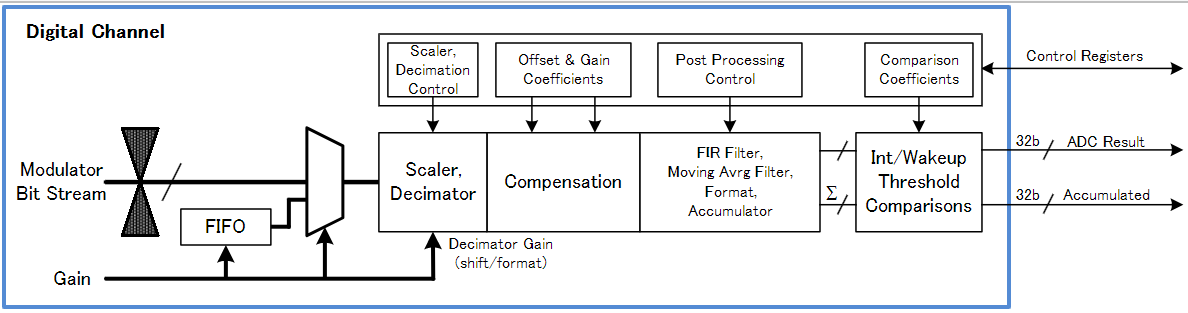
APIs
Cy_Adc_EnableDchan()
cy_en_adc_error_t Cy_Adc_EnableDchan (volatile stc_PACSS_DCHAN_t * base)
Description:
Enables the digital channel
Parameters:
base
– Digital channel base address
Returns:
CY_ADC_ERROR_NONE
if no errors occur
CY_ADC_ERROR_INPUT_ADDRESS_IS_NULL
if
base
is NULL
Cy_Adc_DisableDchan()
cy_en_adc_error_t Cy_Adc_DisableDchan (volatile stc_PACSS_DCHAN_t * base)
Description:
Disables the digital channel
Parameters:
base
– Digital channel base address
Returns:
CY_ADC_ERROR_NONE
if no errors occur
CY_ADC_ERROR_INPUT_ADDRESS_IS_NULL
if
base
is NULL
Cy_Adc_InitDchan()
cy_en_adc_error_t Cy_Adc_InitDchan (volatile stc_PACSS_DCHAN_t * base, cy_stc_adc_dchan_config_t * config)
Description:
Configures the digital channel
Parameters:
base
– Digital channel base address
config
– Configuration options for the digital channel
Returns:
CY_ADC_ERROR_NONE
if no errors occur
CY_ADC_ERROR_INPUT_ADDRESS_IS_NULL
if
base
of
config
is NULL
CY_ADC_ERROR_BAD_PARAM
if
config
contains an invalid parameter
Cy_Adc_ConfigureGainLevel()
cy_en_adc_error_t Cy_Adc_ConfigureGainLevel (volatile stc_PACSS_DCHAN_t * base, cy_stc_adc_gain_level_config_t * gain)
Description:
Configures the digital channel gain level settings
Parameters:
base
– Digital channel base address
gain
– Gain level configuration options for the digital channel
Returns:
CY_ADC_ERROR_NONE
if no errors occur
CY_ADC_ERROR_INPUT_ADDRESS_IS_NULL
if
base
of
config
is NULL
CY_ADC_ERROR_BAD_PARAM
if
config
contains an invalid parameter or if
config
is NULL
Cy_Adc_ ConfigureFIRFilter()
cy_en_adc_error_t ConfigureFIRFilter (volatile stc_PACSS_DCHAN_t * base, cy_stc_adc_fir_config_t * config)
Description:
Configures the digital channel FIR filter coefficients
Parameters:
base
– Digital channel base address
config
– Non-null FIR Filter configuration, which contains:
Post process right shift (FIR right shift)
FIR number of taps
FIR coefficient definitions in an array
Returns:
CY_ADC_ERROR_NONE
if no errors occur
CY_ADC_ERROR_INPUT_ADDRESS_IS_NULL
if
config->coefficients
is NULL
CY_ADC_ERROR_BAD_PARAM
if a filter coefficient field is invalid
Cy_Adc_ConfigureAafMode()
cy_en_adc_error_t Cy_Adc_ConfigureAafMode (volatile stc_PACSS_DCHAN_t * base, cy_stc_adc_dchan_config_t * config)
Description:
Configures the anti-alias filter
Parameters:
base
– Base address
config
– Configuration options for the digital channel
Returns:
CY_ADC_ERROR_NONE
if no errors occur
CY_ADC_ERROR_INPUT_ADDRESS_IS_NULL
if
'base'
of
'config'
is NULL
CY_ADC_ERROR_BAD_PARAM
if
'config'
contains an invalid parameter
On-die temperature sensor
Description
PSoC™ 4 HV PA MCU has an on-die temperature sensor. The measurements are made with an internal temperature sensor by measuring bipolar VBE at different current densities and calculating temperature. Two independent current references are used for diagnosis and redundancy.
APIs
Cy_Adc_EnableTemperature()
cy_en_adc_error_t Cy_Adc_EnableTemperature (volatile stc_PACSS_MMIO_t * base)
Description:
Enables the temperature sensor
Parameters:
base
– PACSS MMIO base address
Returns:
CY_ADC_ERROR_NONE
if no errors occur
CY_ADC_ERROR_INPUT_ADDRESS_IS_NULL
if
base
is NULL
Cy_Adc_DisableTemperature()
cy_en_adc_error_t Cy_Adc_DisableTemperature (volatile stc_PACSS_MMIO_t * base)
Description:
Disables the temperature sensor
Parameters:
base
– PACSS MMIO base address
Returns:
CY_ADC_ERROR_NONE
if no errors occur
CY_ADC_ERROR_INPUT_ADDRESS_IS_NULL
if
base
is NULL
Cy_Adc_InitTemperature()
cy_en_adc_error_t Cy_Adc_InitTemperature (volatile stc_PACSS_MMIO_t * base, cy_stc_adc_temperature_config_t * config)
Description:
Configures the temperature sensor
Parameters:
base
– PACSS MMIO base address
config
– Configuration options for the temperature sensor
Returns:
CY_ADC_ERROR_NONE
if no errors occur
CY_ADC_ERROR_INPUT_ADDRESS_IS_NULL
if
base
is NULL
CY_ADC_ERROR_BAD_PARAM
if
config
contains an invalid parameter
Channel offset and gain calibration
Description
Provides APIs for applying temperature gain and offset correction factors to the DCHAN and AGC. These values are determined in the factory and stored in supervisory flash.
APIs
Cy_Adc_CalibrateAgcGainLevel()
cy_en_adc_error_t Cy_Adc_CalibrateAgcGainLevel (volatile stc_PACSS_MMIO_t * base, uint8_t gainLevel, int32_t temperature, cy_en_adc_achan0_2temp_trim_gain_type_t gain)
Description:
Loads the gain and offset correction values from the supervisory flash
This function calibrates the specified AGC level used in the example code based on the temperature. Calibration must be done after initializing the AGC. Gain and offset calibration values are stored in SFlash as documented in the PACSS calibration section of the TRM.
This function assumes that the gain levels are as configured in the ADC driver. Using a custom gain level setting may affect this function, and could cause the ADC to work improperly.
Parameters:
base
– Address of the PACSS_MMIO registers
gainLevel
– Which AGC Gain Level to calibrate. Ranges from 0 to 8
temperature
– Fixed point, 12.20, junction temperature in celsius
gain
– Gain Level of the selected PACSS_MMIO Gain Level. Options are:
CY_ADC_ACHAN0_2TEMP_GAIN_2X
CY_ADC_ACHAN0_2TEMP_GAIN_4X
CY_ADC_ACHAN0_2TEMP_GAIN_8X
CY_ADC_ACHAN0_2TEMP_GAIN_16X
CY_ADC_ACHAN0_2TEMP_GAIN_32X
CY_ADC_ACHAN0_2TEMP_GAIN_64X
CY_ADC_ACHAN0_2TEMP_GAIN_128X
CY_ADC_ACHAN0_2TEMP_GAIN_256X
CY_ADC_ACHAN0_2TEMP_GAIN_512X
Returns:
CY_ADC_ERROR_NONE if no errors occur
CY_ADC_ERROR_BAD_PARAM
if
gainLevel
,
gain
, or
sampleRate
are invalid
CY_ADC_ERROR_INPUT_ADDRESS_IS_NULL
if
base
is NULL
Cy_Adc_CalibrateAchan0_2TempTrim()
cy_en_adc_error_t Cy_Adc_CalibrateAchan0_2TempTrim (volatile stc_PACSS_DCHAN_t * base, cy_en_adc_achan0_2temp_trim_gain_type_t gain, int32_t temperature)
Description:
Loads the gain and offset correction values from the supervisory flash
This function loads the gain and offset correction values for the specified DCHAN connected to ACHAN0.
The output of the DCHAN must have the same LSB at the application of OCOR as the configuration used to create the values stored in supervisory flash. This can be accomplished by adjusting either SHIFTL or
DEC_SHIFTR
.
The
Cy_Adc_GetDieTempFromDelta
API calculates the junction temperature in this fixed-point format from the difference between two die temperature measurements. This function uses the
Cy_Adc_GetGcorOcorAchan0_2TempTrim
API to perform a linear interpolation of the OCOR and GCOR values in the supervisory flash based on the provided temperature.
DCHAN connected to ACHAN0. This function uses the
Cy_Adc_GetGcorOcorAchan0_2TempTrim
API to perform a linear interpolation based on the provided temperature. 2Temp means the interpolation is done using a 2-point array.
Parameters:
base
– Address of the DCHAN registers
gain
– Gain value of the specified channel. Options are:
CY_ADC_ACHAN0_2TEMP_GAIN_1X
CY_ADC_ACHAN0_2TEMP_GAIN_2X
CY_ADC_ACHAN0_2TEMP_GAIN_4X
CY_ADC_ACHAN0_2TEMP_GAIN_8X
CY_ADC_ACHAN0_2TEMP_GAIN_16X
CY_ADC_ACHAN0_2TEMP_GAIN_32X
CY_ADC_ACHAN0_2TEMP_GAIN_64X
CY_ADC_ACHAN0_2TEMP_GAIN_128X
CY_ADC_ACHAN0_2TEMP_GAIN_256X
CY_ADC_ACHAN0_2TEMP_GAIN_512X
temperature
– Fixed point, 12.20, junction temperature in celsius
Returns:
CY_ADC_ERROR_NONE
if no errors occur
CY_ADC_ERROR_BAD_PARAM
if
gain
or
sampleRate
are invalid
CY_ADC_ERROR_INPUT_ADDRESS_IS_NULL
if
base
is NULL
Cy_Adc_CalibrateAchan1_2TempTrim()
cy_en_adc_error_t Cy_Adc_CalibrateAchan1_2TempTrim (volatile stc_PACSS_DCHAN_t * base, cy_en_adc_achan1_2temp_trim_gain_type_t gain, int32_t temperature)
Description:
Loads the gain and offset correction values from the supervisory flash
This function loads the gain and offset correction values for the specified DCHAN connected to ACHAN1.
The output of the DCHAN must have the same LSB at the application of OCOR as the configuration used to create the values stored in the supervisory flash. This can be accomplished by adjusting either SHIFTL or
DEC_SHIFTR
.
The
Cy_Adc_GetDieTempFromDelta
API calculates the junction temperature in this fixed point format from the difference between two die temperature measurements. This function uses the
Cy_Adc_GetGcorOcorAchan1_2TempTrim
API to perform a linear interpolation of the OCOR and GCOR values in supervisory flash based on the provided temperature.
DCHAN connected to ACHAN1. This function uses the
Cy_Adc_GetGcorOcorAchan1_2TempTrim
API to perform a linear interpolation based on the provided temperature. 2Temp means the interpolation is done using a 2-point array.
Parameters:
base
– Address of the DCHAN registers
gain
– Gain value of the specified channel. Options are:
CY_ADC_ACHAN1_2TEMP_GAIN_0P5X
CY_ADC_ACHAN1_2TEMP_GAIN_1X
CY_ADC_ACHAN1_2TEMP_GAIN_2X
CY_ADC_ACHAN1_2TEMP_GAIN_4X
CY_ADC_ACHAN1_2TEMP_GAIN_8X
CY_ADC_ACHAN1_2TEMP_GAIN_16X
CY_ADC_ACHAN1_2TEMP_GAIN_32X
CY_ADC_ACHAN1_2TEMP_GAIN_64X
CY_ADC_ACHAN1_2TEMP_GAIN_128X
CY_ADC_ACHAN1_2TEMP_GAIN_256X
CY_ADC_ACHAN1_2TEMP_GAIN_512X
temperature
– Fixed point, 12.20, junction temperature in celsius
Returns:
CY_ADC_ERROR_NONE
if no errors occur
CY_ADC_ERROR_BAD_PARAM
if
gain
or
sampleRate
are invalid
CY_ADC_ERROR_INPUT_ADDRESS_IS_NULL
if
base
is NULL
Cy_Adc_CalibrateAchan1_3TempTrim()
cy_en_adc_error_t Cy_Adc_CalibrateAchan1_3TempTrim (volatile stc_PACSS_DCHAN_t * base, cy_en_adc_achan1_3temp_trim_divider_type_t divider, int32_t temperature)
Description:
Loads the gain and offset correction values from the supervisory flash
This function loads the gain and offset correction values for the specified DCHAN connected to ACHAN1. These values are for the high-voltage divider measurements.
The output of the DCHAN must have the same LSB at the application of OCOR as the configuration used to create the values stored in the supervisory flash. This can be accomplished by adjusting either SHIFTL or
DEC_SHIFTR
.
The
Cy_Adc_GetDieTempFromDelta
API calculates the junction temperature in this fixed-point format from the difference between two die temperature measurements. This function uses the
Cy_Adc_GetGcorOcorAchan1_2TempTrim
API to perform a linear interpolation of the OCOR and GCOR values in supervisory flash based on the provided temperature. measurements. This function uses the
Cy_Adc_GetGcorOcorAchan1_2TempTrim
API to perform a linear interpolation based on the provided temperature. 3Temp means the interpolation is done using a 3-point array.
Parameters:
base
– Address of the DCHAN registers
divider
– Which high-voltage divider is being sampled by the DCHAN. Options are:
CY_ADC_ACHAN1_3TEMP_VSENSE_16
CY_ADC_ACHAN1_3TEMP_VSENSE_24
CY_ADC_ACHAN1_3TEMP_VDIAG_16
CY_ADC_ACHAN1_3TEMP_VDIAG_24
temperature
– Fixed point, 12.20, junction temperature in celsius
Returns:
CY_ADC_ERROR_NONE
if no errors occur
CY_ADC_ERROR_BAD_PARAM
if
divider
or
sampleRate
are invalid
CY_ADC_ERROR_INPUT_ADDRESS_IS_NULL
if
base
is NULL
Cy_Adc_GetGcorOcorAchan0_2TempTrim()
cy_en_adc_error_t Cy_Adc_GetGcorOcorAchan0_2TempTrim (uint16_t *gcor, int16_t *ocor, cy_en_adc_achan0_2temp_trim_gain_type_t gain, int32_t temperature)
Description:
Retrieves the gain and offset correction values from the supervisory flash
This function loads the gain and offset correction values for the specified gain level. This function performs a linear interpolation of the gain and offset correction values based on the values defined for -40°C and 150°C. 2Temp means the interpolation is done using a 2-point array.
Parameters:
gcor
– Pointer to the gain correction value
ocor
– Pointer to offset correction value
gain
– Gain value of the specified channel
temperature
– Fixed-point, 12.20, junction temperature in celsius
Returns:
CY_ADC_ERROR_NONE
if no errors occur
CY_ADC_ERROR_BAD_PARAM
if
gain
is invalid
CY_ADC_ERROR_INPUT_ADDRESS_IS_NULL
if
base
is NULL
Cy_Adc_GetGcorOcorAchan1_2TempTrim()
cy_en_adc_error_t Cy_Adc_GetGcorOcorAchan1_2TempTrim (uint16_t *gcor, int16_t *ocor, cy_en_adc_achan1_2temp_trim_gain_type_t gain, int32_t temperature)
Description:
Retrieves the gain and offset correction values from the supervisory flash
This function loads the gain and offset correction values for the specified gain level. This function performs a linear interpolation of the gain and offset correction values based on the values defined for -40°C and 150°C. 2Temp means the interpolation is done using a 2-point array.
Parameters:
gcor
– Pointer to the gain correction value
ocor
– Pointer to offset correction value
gain
– Gain value of the specified channel
temperature
– Fixed-point, 12.20, junction temperature in celsius
Returns:
CY_ADC_ERROR_NONE
if no errors occur
CY_ADC_ERROR_BAD_PARAM
if
gain
is invalid
CY_ADC_ERROR_INPUT_ADDRESS_IS_NULL
if
base
is NULL
Cy_Adc_GetGcorOcorAchan1_3TempTrim()
cy_en_adc_error_t Cy_Adc_GetGcorOcorAchan1_3TempTrim (uint16_t *gcor, int16_t *ocor, cy_en_adc_achan1_3temp_trim_divider_type_t divider, int32_t temperature)
Description:
Retrieves the gain and offset correction values from the supervisory flash
This function loads the gain and offset correction values for the specified gain level. 3Temp means the interpolation is done using a 3-point array.
Parameters:
gcor
– Pointer to the gain correction value
ocor
– Pointer to offset correction value
gain
– Gain value of the specified channel
temperature
– Fixed point, 12.20, junction temperature in celsius
Returns:
CY_ADC_ERROR_NONE
if no errors occur
CY_ADC_ERROR_BAD_PARAM
if
gain
is invalid
CY_ADC_ERROR_INPUT_ADDRESS_IS_NULL
if
base
is NULL
Cy_Adc_CalibrateOffsetScalar()
cy_en_adc_error_t Cy_Adc_CalibrateOffsetScalar (volatile stc_PACSS_DCHAN_t * base)
Description:
Loads the offset correction scalar value from the supervisory flash
This function loads the offset correction scalar value for the specified DCHAN.
Parameters:
base
– Address of the DCHAN registers
Returns:
CY_ADC_ERROR_NONE
if no errors occur
CY_ADC_ERROR_INPUT_ADDRESS_IS_NULL
if
base
is NULL
Convert raw ADC counts to volts
Description
Provides APIs for converting ADC counts to volts and millivolts. This is to show the basic functionality of the evaluation board with easily understood the results that would match a voltmeter measuring the board. Results are in floating-point format which will lose precision for large integer values. It is up to the user to prevent this in their application.
APIs
Cy_Adc_CountsToVolts()
float Cy_Adc_CountsToVolts (int32_t counts, cy_en_adc_channel_type_t channelType, cy_en_adc_sample_rate_t sampleRate, float vref)
Description:
Converts the input from raw ADC counts to volts
ADC counts are explained in the decimator result calculation section of the TRM. Some of that explanation is replicated here along with an example of how the results correlate to voltage.
The ADC result depends on the following parameters:
M = modulator data, ranges from -4 to 4
S = Scaler, left shift ranges from 0 to 9 (SHIFTL)
N = Number of sinc stages, values of 3 or 4 (SINC_MODE)
DR = Decimation ratio, typical values are: 32, 64 or 128
U = Moving sum (disabled: disabled = 1, two taps: U=2, four taps: U=4)
DR2 = Rate reducer decimation ratio; typical values: 2 or 6
OF = Offset correction (OCOR)
OFS = Offset scaler (OCOR_SCLR)
G = Gain correction (GCOR)
GV = Gain correction valid bits (GVAL)
RSA = Decimator right shift (DEC_SHIFTR)
RSB = Rate reducer right shift (RR_SHIFT)
To simplify the calculation, these steps assume that moving average is disabled, and the modulator data input is constant.
The result is calculated using the following calculations:
sinc3/sinc4 results = A = (M << S) * 2^(N*log2(DR)) * U
right shift result = B = A >> RSA
offset result = C = B + (OF << OFS)
gain result = D = (C * G) >> GV
sinc2 result = E = D * 2^(2*log2(DR2))
decimator output = F = E >> RSB
The left shift is most commonly used in AGC to keep all results on the same number scale regardless of gain level. Right shifts are used to prevent overflowing the 32-bit result register.
Note: When using a Moving Sum of 4, subtract 30 instead of 32 from the equations below:
The equation for determining DEC_SHIFTR is:
log2(qlev) + max(SHIFTL) + N*log2(DR) - 30
Where qlev = 9, the quantization levels of the modulator -4 to 4, including 0.
The equation for determining RR_SHIFTR is:
log2(qlev) + max(SHIFTL) + Nlog2(DR +1) +2log2(DR2+1) - DEC_SHIFTR - 30
The maximum output value, MAX_COUNT below, is determined by using the maximum modulator output which is 4. Similarly, the minimum modulator output value is -4 so the MIN_COUNT == MAX_COUNT * -1. The LSB is the reference voltage divided by MAX_COUNT.
The code examples use three different configurations, and will walk through the MAX_COUNT calculation for the current channel and provide the parameters for the other channels. The current channel uses a SHIFTL of 8 at the lowest AGC gain setting with SHIFTL decreasing with each gain increase to keep the values on the same scale.
For this exercise, assume that offset and gain correction are used to keep the results along the ideal, linear curve between +/- VREF. Therefore, you can ignore the gain and offset calculations (steps 3 and 4 above).
Current channel
SHIFTL = 8
DR = 64
N = 3 (Sinc3, SINC_MODE=0)
DEC_SHIFTR = log2(qlev) + max(SHIFTL) + N*log2(DR) - 30
= log2(9) + max(8) + 3*log2(64) - 30
= 3.17 + 8 + 18 - 30
= 29.17 - 30
= -0.83, rounded to the nearest positive integer
= 0
DR2 = 6
RR_SHIFTR = log2(9) + max(SHIFTL) + Nlog2(DR) + 2log2(DR2) - DEC_SHIFTR - 30
= 3.17 + 8 + 18 + 2*log2(6) - 0 - 30
= 29.17 + 5.17 - 30
= 34.34 - 30
4.34, rounded to the nearest positive integer
= 5
MAX COUNT = (DECB * 2^(2*log2(DR2))) >> RR_SHIFTR, where:
DECB = ((4 << SHIFTL)2^(Nlog2(DR)) * U >> DEC_SHIFTR)
DECB = ((4 << 8)2^(3log2(64) * 4) >> 0)
DECB = 1024 *2^18 * 4 >> 0
DECB = 1073741824
= (DECB) * 2^(2*log2(6)) >> 5
= 1073741824 * 2^5.1699 >> 5
= 1,207,959,552 (0x48000000)
The current channel uses AGC with gains of 0.5x to 128x as well as an accumulated average (U) of 4x. This means that the lowest AGC gain is effectively 2x (0.5x gain * 4x summed average). To compensate for this 2x gain in the equations below, subtract one from the RR_SHIFTR calculated above, making it 4.
Voltage channel
SHIFTL = 0
DR = 64
DEC_SHIFTR = 0
DR2 = 6
RR_SHIFTR = log2(9) + max(0) + 3log2(64) + 2log2(6) - 0 - 30
= 3.17 + 18 + 5.17 -30
= -3.66
= 0
MAX COUNT = 37,748,736(0x02400000)
Diagnostic channel
SHIFTL = 0
DR = 64
DEC_SHIFTR = 0
DR2 = 1
RR_SHIFTR = 0
MAX COUNT = 1,048,576 (0x00100000)
Voltage output:
voltage = decimator_output * ((max_reference_voltage - min_reference_voltage) / (max_counts - min_counts))
Parameters:
counts
– ADC Results from the conversion to be converted to millivolts
channelType
– Channel type. Options are:
CY_ADC_CURRENT_CHANNEL
CY_ADC_VOLTAGE_CHANNEL
CY_ADC_DIAGNOSTIC_CHANNEL
sampleRate
– Channel sample rate. Options are:
CY_ADC_SAMPLE_RATE_48KSPS
CY_ADC_SAMPLE_RATE_8KSPS
CY_ADC_SAMPLE_RATE_4KSPS
CY_ADC_SAMPLE_RATE_3KSPS
CY_ADC_SAMPLE_RATE_2KSPS
CY_ADC_SAMPLE_RATE_1KSPS
vref
– Reference voltage in Volts
Returns:
Floating-point value of the result in volts
Cy_Adc_CountsToMillivolts()
float Cy_Adc_CountsToMillivolts (int32_t counts, cy_en_adc_channel_type_t channelType, cy_en_adc_sample_rate_t sampleRate, float vref)
Description:
Converts the input from raw ADC counts to millivolts
Voltage output:
voltage = decimator_output * ((max_reference_voltage - min_reference_voltage) / (max_counts - min_counts))
Parameters:
counts
– ADC Results from the conversion to be converted to millivolts
channelType
– Channel type. Options are:
CY_ADC_CURRENT_CHANNEL
CY_ADC_VOLTAGE_CHANNEL
CY_ADC_DIAGNOSTIC_CHANNEL
sampleRate
– Channel sample rate. Options are:
CY_ADC_SAMPLE_RATE_48KSPS
CY_ADC_SAMPLE_RATE_8KSPS
CY_ADC_SAMPLE_RATE_4KSPS
CY_ADC_SAMPLE_RATE_3KSPS
CY_ADC_SAMPLE_RATE_2KSPS
CY_ADC_SAMPLE_RATE_1KSPS
vref
– Reference voltage in volts
Returns:
Floating-point value of the result in millivolts
On-die temperature calculation
Description
Provides APIs for converting an ADC count delta to a temperature value.
APIs
Cy_Adc_GetDieTempFromDelta()
cy_en_adc_error_t Cy_Adc_GetDieTempFromDelta(int32_t *result, int32_t delta, cy_en_adc_die_temp_setup_t setup)
Description:
Converts the delta between two die temp measurements to degrees celsius in fixed-point 12.20 format
Uses the formula (a2 * x^2 * 2^-34 + a1 * x * 2^-9 + a0 * 2^14)/2^20
where x = Delta ADC = ADC(UNIT) - ADC(1)
The division by 2^20 is not performed; it is symbolic of the fixed-point 12.20 format of the result.
Parameters:
delta
– 32-bit delta between the two die temp measurements
result
– Pointer for the conversion result in fixed-point 12.20 format
setup
– Selects the primary or alternate temperature measurement coefficients stored in SFlash
Returns:
CY_ADC_ERROR_NONE
if no errors occur
CY_ADC_ERROR_BAD_PARAM
if
delta
is invalid
CY_ADC_ERROR_INPUT_ADDRESS_IS_NULL
if
result
is NULL
Cy_Adc_InitializeDieTempConfigs()
cy_en_adc_error_t Cy_Adc_InitializeDieTempConfigs (cy_stc_adc_temperature_config_t * one, cy_stc_adc_temperature_config_t * unit, cy_en_adc_die_temp_setup_t setup)
Description:
Initializes the two configurations used for temperature measurement with factory settings.
Die temperature measurements are made by taking two measurements, ADC(1) and ADC(UNIT). Each measurement uses a different number of either bipolar units or reference currents. The difference of these two measurements can be converted to a temperature using the
Cy_Adc_GetDieTempFromDelta
API.
Parameters:
one
– Address of the configuration for the (1) measurement
unit
– Address of the configuration for the (UNIT) measurement
setup
– Selects the primary or alternate temperature measurement parameters stored in SFlash
Returns:
CY_ADC_ERROR_NONE
if no errors occur
CY_ADC_ERROR_BAD_PARAM
if
setup
in invalid
CY_ADC_ERROR_INPUT_ADDRESS_IS_NULL
if
one
or
unit
are NULL
Cy_Adc_NormalizeDelta()
cy_en_adc_error_t Cy_Adc_NormalizeDelta(int32_t *newDelta, int32_t delta, float ratio)
Description:
Normalizes the delta VBE measurement to the ratio of the current sources.
The delta VBE measurement is normalized to the ratio of the current sources by measuring the resistive load of the temperature sensor using the same bipolar transistors and current units.
The ratio of current sources or transistors is usually 9/1 so normalization can be done with the equation:
newDelta = delta*LN(9)/LN(ratio)
Natural logarithm is processor intensive so we instead use the linear approximation:
newDelta = delta + delta*(A*ratio + B)
where A = -0.0534 and B = 0.48
Parameters:
newDelta
– Address to store the normalized delta VBE
delta
– Delta VBE determined by two ADC measurements
ratio
– UNIT/1 ratio of the measured voltage across the resistor
Returns:
CY_ADC_ERROR_NONE
if no errors occur
CY_ADC_ERROR_BAD_PARAM
if
setup
in invalid
CY_ADC_ERROR_INPUT_ADDRESS_IS_NULL
if
one
or
unit
are NULL
Shunt resistor open detection of RSx pins
Description
Provides APIs for detecting disconnect shunt connections by switching internal pull-up resistors to the shunt pins. If the resistance between the RSHx or RSLx to ground is more than 1000 Ω, an open pin fault can be detected.
Figure 23
shows the shunt resistor open detection diagram.
Figure 23. Shunt resistor open detection diagram
APIs
Cy_Adc_GetPullupResistance()
uint16_t Cy_Adc_GetPullupResistance (cy_en_adc_rs_pin_type_t pin, int32_t temperature)
Description:
Returns the linearly interpolated resistance of the pull-up resistor
Parameters:
pullup
– Selects which of the diagnostic pull-up resistors to choose
temperature
– Temperature of the die in 12.20 fixed-point celsius. Used for linear interpolation of the pull-up value along with the hot and cold values stored in the SFlash
Returns:
uint16_t
Pull-up resistance value in ohms; returns zero if
pull-up
is invalid
Cy_Adc_IsRsOpen()
bool Cy_Adc_IsRsOpen (int32_t pullup, int32_t shunt, int32_t temperature, cy_en_adc_rs_pin_type_t pin)
Description:
Uses samples of the shunt resistor and pull-up resistor to determine if the shunt resistor is disconnected (open). The circuit is open if the measured voltage with the pull-up enabled (Vpu) is greater than 1 volt or if Vpu > Vadc_th where Vadc_th is:
Vadc_th = Vsh + (Vdd - Vsh) * 600 / (600 + Rpu)
Vsh is the measured shunt voltage Rpu is the value of the pull-up resistor, determined using the temperature, based on measured values stored in SFlash.
The diagnostic channel uses a gain of 0.5x for these samples. The values input is multiplied by 2 in this function to correct for that attenuation.
Parameters:
pullup
– Result of measuring with the pull-up resistor enabled
shunt
– Result of measuring the shunt without the pull-up
temperature
– Temperature of the die in 12.20 fixed point celsius. Used to determine the pull-up value
pin
– Selects which pin is being tested
Returns:
true if RS open detected
false if RS open not detected
Summary
This application note had guided you details of the precision analog channel subsystem of PSoC™ 4 HV PA MCU. By using the precision analog channel subsystem, battery monitoring and management applications can be achieved with higher precision and a small number of external components. Infineon provides an evaluation board and wealth of sample software to help you get started with PSoC™ 4 HV PA family MCUs. To evaluate the evaluation board, contact your sales representative or Infineon Technical Support.
Glossary
Terms | Description |
|---|---|
AAF | anti-alias filter |
ACHAN | analog channel |
A/D converter | analog to digital converter |
ADC | analog to digital converter |
AGC | auto gain correction or auto gain control |
AHB | advanced high-performance bus |
API | application programming interface |
BOD | brown-out detectors |
CM0+ | Arm® Cortex®-M0+ (processor core name) |
CPU | central processing unit |
CPUSS | CPU subsystem |
DAP | debug access port |
DCHAN | digital channel |
DMA | direct memory access |
DMAC | DMA controller |
DR | decimation rate or decimation ratio |
DSM | delta-sigma modulator |
DW | data wire |
ECC | error correction code (safety) |
ESD | electro-static discharge |
FIR | finite impulse response |
FW | firmware |
GCOR | gain correction |
GPIO | general purpose I/O |
HPBGR | high-precision bandgap reference |
HV | high-voltage |
HW | hardware |
I/O | input or otput |
IAR | IAR Systems (company name) |
IOSS | I/O subsystem |
IRC | interrupt controller |
IRQ | interrupt request |
ISR | interrupt service routine |
LDO | low dropout |
LIN | local interconnect network |
LSB | least significant bit |
MCU | microcontroller unit |
MIPI | mobile industry processor interface |
MMIO | memory-mapped peripheral I/O |
MPU | memory protection unit |
MSB | most significant bit |
NMI | non-maskable interrupt |
NTC | negative temperature coefficient |
OCOR | offset correction |
PA | precision analog |
PACSS | precision analog channel subsystem |
PGA | programmable gain amplifier |
POR | power on reset |
PWM | pulse width modulation |
RAM | random access memory |
ROM | read-only memory |
SCB | serial communication block |
SDL | sample driver library |
SPI | serial peripheral interface |
SFLASH | supervisory flash |
SRAM | static RAM |
SRSS | system resource subsystem |
SWD | serial wire debugging |
TCPWM | timer, counter and PWM |
TRM | technical reference manual |
TVS | transient voltage suppressors |
UART | universal asynchronous receiver transmitter |
VDIVIDER | voltage divider |
WDT | watchdog timer |
References
The following are the PSoC™ 4 HV PA family series application notes, datasheets and technical reference manuals. Contact
Technical Support
to obtain these documents and sample driver library.
Application notes
AN230264 - Getting started with PSoC™ 4 HV PA family
AN230265 - Hardware design guide for PSoC™ 4 HV PA family
AN230371 - High voltage subsystem (HVSS) in PSoC™ 4 HV PA family
Device datasheet
PSoC™ 4 HV precision analog datasheet
Architecture reference manual
PSoC™ 4 HV PA architecture reference manual (RM)
Registers reference manual
PSoC™ 4 HV PA registers reference manual (RM)
Evaluation board user guide
PSoC™ 4 HV PA evaluation board user guide
Sample driver library (SDL)
PSoC™ 4 HV PA sample driver library
Revision history
Document version | Date of release | Description of changes |
|---|---|---|
** | 2021-11-25 | Initial release |
*A | 2023-04-19 | Template update; no content updated. |