About this document
Scope and purpose
AN230264 briefly introduces you to PSOC™ high-voltage (HV) precision analog (PA) family, an Arm® Cortex®-M0+ based microcontroller. This application note also guides you to set up the PSOC™ HV PA development environment.
Intended audience
This document is intended for anyone using PSOC™ HV PA family MCUs.
Introduction
This application note provides an overview of the device feature set, and describes the development environment and tools to get started with the CY8C41xxLCE-HV4xx series from the PSOC™ HV PA family. PSOC™ HV PA is a fully integrated programmable embedded system for battery monitoring and management. The system features an Arm® Cortex® M0+ processor with programmable and reconfigurable analog and digital blocks. The PSOC™ HV PA will be offered in a 32-QFN package with wettable flanks. To get a better understanding of the functionality described and terminology used in this application note, see "Section A: Overview" of the architecture technical reference manual (architecture TRM) 2.
Feature set
PSOC™ HV PA is a fully integrated programmable embedded system for battery monitoring and management. The system features an Arm® Cortex® M0+ processor, and programmable and reconfigurable analog and digital blocks.
PSOC™ HV PA devices have these characteristics:
- High-performance, 24 to 49.152-MHz Arm® Cortex® M0+ CPU with MPU and DMA controller
- Precision analog channel subsystem (PACSS)
- High voltage subsystem (tolerant up to 42 V)
- Integrated LIN transceiver
- High-precision clock sources
- Configurable Timer Counter PWM (TCPWM) block
- Configurable Serial Communication Block (SCB) with I2C, SPI, UART, and LIN slave operating modes
- Low-power operating modes: Sleep and Deep Sleep
- Functional safety for ASIL-B according to ISO 26262
- Automotive Electronics Council (AEC) AEC-Q100 qualified
Figure 1 shows the major components of the PSOC™ HV PA architecture.
Function summary
- 32-bit CPU subsystem
- Up to 49.152-MHz Arm® Cortex® M0+ CPU with MPU and DMA controller
- Up to 128 KB of code flash with ECC
- Up to 8 KB of SRAM with ECC
- Up to 8 KB of data flash with ECC
- Precision analog channel subsystem (PACSS)
- Two precision delta-sigma ADCs (16-20+ bits)
- Current channel with automatic gain
- Voltage channel
- Temperature and diagnostic channels
- Digital filtering, accumulators, and threshold comparisons on all channels
- High-voltage subsystem
- Operates directly off 12 V/24 V battery (tolerant up to 42 V)
- Integrated LIN transceiver
- HV input divider for voltage channel
- Functional safety for ASIL-B
- Development process of ISO 26262 for ASIL B
- Memory protection unit (MPU)
- Challenge-response watchdog timer (CRWDT)
- Overvoltage protection (OVP) and brownout detection (BOD)
- Hardware error correction (SECDED ECC)
- Analog diagnostics
- Timing and pulse-width modulation
- Four 16-bit TCPWM blocks
- Center-aligned, edge, and pseudo-random modes
- Quadrature decoder
- Clock Sources
- ±2% up to 49.152 MHz internal main oscillator (IMO)
- ±1% 2 MHz High-precision oscillator (HPOSC)
- 40-kHz Internal low-speed oscillator (ILO)
- ±5% or ±7% 32-kHz precision low-power oscillator (PILO) based on the part number
- Communication
- SCBs with re-configurable I2C, SPI, UART, or LIN slave
- LIN interface compliant with LIN 2.2 A and ISO 17987 standards
- Up to 8 GPIOs
- Package
- 32-QFN with wettable flanks (6 x 6 mm)
Development environment and tools
Evaluation board
The CYHVPA-128K-32-001 Evaluation Board (Figure 2) provides access to all peripherals, resulting in a fully featured evaluation platform. CYHVPA-128K-32-001 has Arm® standard MIPI 10-pin / 20-pin connectors for the debug interface by third-party interfaces, and Infineon KitProg3 low-level communication interface for programming and debugging. The evaluation board can be used for the development of software. For more information on board details, see the PSOC™ HV PA Evaluation Board user guide 4.
Figure 3 shows the CYHVPA-128K-32-001 Evaluation Board block diagram.
CYHVPA-128K-32-001 board connections
| CY8C4147LCE-HV413 (U3) | Connection/component | |
|---|---|---|
|
Pin |
Pin name |
|
|
1 |
VDDA |
Internal analog power (3.3 V): 0.15 μF capacitor |
|
2 |
VSSA |
Analog GND |
|
3 |
RSH2 |
100 μ / 50 μΩ shunt resistor |
|
4 |
RSH |
100 m / 75 m / 50 m / 4.02 Ω shunt resistor |
|
5 |
RSL |
100 m / 75 m / 50 m / 4.02 Ω shunt resistor |
|
6 |
RSL2 |
100 μ / 50 μΩ shunt resistor |
|
7 |
VSSA |
Analog GND |
|
8 |
VREFH |
0.47 μF capacitor + side |
|
9 |
VREFL |
0.47 μF capacitor - side |
|
10 |
VTEMP_RET |
Thermistor or potentiometer |
|
11 |
VTEMP |
Thermistor or potentiometer |
|
12 |
VTEMP_SUP |
33 kΩ resistor |
|
13 |
VSSD |
Digital GND |
|
14 |
XRES |
Reset switch / program connector |
|
15 |
P0[7] |
SWDCLK for programming |
|
16 |
P0[6] |
SWDIO for programming |
|
17 |
P0[5] |
User push switch / I/O header |
|
18 |
P0[4] |
User DIP switch / I/O header |
|
19 |
P0[3] |
User LED (green) / I/O header |
|
20 |
P0[2] |
User LED (red) / I/O header |
|
21 |
P0[1] |
I2C SDA / UART TX / I/O header |
|
22 |
P0[0] |
I2C SCL / UART RX / I/O header |
|
23 |
VCCD |
Internal digital power (1.8 V): 0.15 μF capacitor |
|
24 |
VDDD |
Internal digital power (3.3 V): 0.1 μF, 3.3 μF capacitors |
|
25 |
VSSD |
Digital GND |
|
26 |
VSSL |
LIN GND |
|
27 |
NC1 |
- |
|
28 |
LIN |
LIN connector |
|
29 |
NC2 |
- |
|
30 |
VDIAG |
VBAT voltage sensing with 2.2 kΩ resistor (for diagnostic) |
|
31 |
VSENSE |
VBAT voltage sensing with 2.2 kΩ resistor |
|
32 |
VBAT |
12 V power supply input |
|
- |
EPAD |
Heat pad (GND) |
Connection diagram with tools
PSOC™ HV PA has an SWD interface to connect with third-party debuggers. The debug pin of SWD is shared with the GPIO port (P0[6] and P0[7]). For more information, see AN230265 - Hardware design guide for PSOC™ HV PA family. Figure 4 and Figure 5 show an example of the basic connection for PSOC™ HV PA devices. Note that the external resistors are optional.
Automotive Peripheral Driver Library (AutoPDL)
Automotive Peripheral Driver Library (AutoPDL) provides ISO 26262-compliant low-level drivers for all PSOC™4 HV peripherals.
The development environment officially supported by AutoPDL is IAR EWARM. To use EWARM, obtain the appropriate license. See Peripheral drivers for information regarding the software and license.
CPU (CM0+) startup sequence for PSOC™ HV PA
The following steps are involved in the device startup sequence:
- System reset (at 0x0000 0000)
- CM0+ in SROM/boot
- Device in privilege mode
- Perform trimming of the device based on the 64-bit key
- SWD initialized
- APIs executed from Arm® CM0+ NMI
- APIs for the flash program, erase, and read
- APIs to retrieve data from privilege registers
- Transfer control to the user program
- Device in user mode
- CM0+ executes the user application from the code flash region
The following steps are involved in the application startup sequence:
- System reset (at 0x0000 0000).
- CM0+ executes "SystemInit"
- Disables WDT
- Applies flash wait states
- Clock selection
- Enables generic system IRQ
- Continues execution of CM0+ user application
Startup flow example
The application startup sequence process is executed after the boot process completes. In the boot process, according to the lifecycle stage, protection status and debug access restriction settings are mainly performed, and application authentication is performed. In the application startup sequence process, initial settings necessary for program execution such as disabling the WDT, applying flash wait state, and clock settings are completed, and then execution jumps to the main routine. CM0+ executes the boot code after reset.
Figure 6 describes the PSOC™ HV PA device startup flow.
Sample code
Code Listing 1 Sample code for CM0+ startup and Code Listing 2 Sample code for CM0+ main function show a sample code for the CM0+ startup and main function respectively.
Code Listing 1 Sample code for CM0+ startup
;************************************************************************
;* Start-up Code
;************************************************************************
      THUMB
      PUBWEAK Reset_Handler
      SECTION .text:CODE:REORDER:NOROOT(2)
Reset_Handler:

; Disable global interrupts
      CPSID   I

; Update Vector Table Offset Register with address of user ROM table
; (will be updated later to user RAM table address in C startup code)
      LDR  r0, =__vector_table
      LDR  r1, =VTOR
      STR  r0, [r1]
      DSB

; Initialize ECC of startup stack (needed for local variables in C startup code) by processing 8 bytes per loop iteration,

; Prerequisite: Stack Pointer (SP) has not been modified (from the vector table init value) by above code (otherwise code must be adapted)
      MOVS r0, #0 ; clear value
      MOVS r1, #0 ; clear value
      LDR  r2, Cy_u32StartupStackStartAddress
startup_stack_ecc_init_loop:
      STM  r2!, {r0, r1}
      CMP  r2, sp
      BNE  startup_stack_ecc_init_loop

; Call C startup code (no ANSI C context established yet!)
      LDR  r7, =Startup_Init
      BLX  r7

; Initialize data sections
      LDR  r7, =__iar_data_init3
      BLX  r7

      LDR  r7, =__iar_program_start
      BLX  r7

; Note: Control flow does not necessarily return here.
; On some tool-chains (e.g. IAR) control flow will never return from
; the system library.
Cy_Main_Exited:
      B    Cy_Main_Exited
Code Listing 2 Sample code for CM0+ main function
#include "intrinsics.h" /* To use IAR embedded function */
#include "startup.h"
#include "bb_bsp.h"
#include "cy_common_def.h"
#include "cy_error_callout.h"
#include "cy_gpio.h"
#include "cy_sysclk.h"
#include "cy_syslib.h"
int main(void)
{
uint8 flag = 1;
SystemInit();
__enable_interrupt(); /* Enable global interrupts. */
/* Initialize USER LED1 port/pin */
Cy_Gpio_SetPinMode(CY_USER_LED1_PORT_IDX, CY_USER_LED1_PIN, CY_USER_LED1_MUX);
Cy_Gpio_SetDriveMode(CY_USER_LED1_PORT_IDX, CY_USER_LED1_PIN,
CY_GPIO_DRIVE_MODE_STRONG);
/* Initialize USER LED2 port/pin */
Cy_Gpio_SetPinMode(CY_USER_LED2_PORT_IDX, CY_USER_LED2_PIN, CY_USER_LED2_MUX);
Cy_Gpio_SetDriveMode(CY_USER_LED2_PORT_IDX, CY_USER_LED2_PIN,
CY_GPIO_DRIVE_MODE_STRONG);
for(;;)
{ // Wait 0.05 [s]
Cy_SysLib_DelayUs(50000);
switch(flag)
{
case 1:
Cy_Gpio_Inv(CY_USER_LED1_PORT_IDX, CY_USER_LED1_PIN);
flag = 2;
break;
case 2:
Cy_Gpio_Inv(CY_USER_LED2_PORT_IDX, CY_USER_LED2_PIN);
flag = 1;
break;
default:
Cy_Gpio_Inv(CY_USER_LED1_PORT_IDX, CY_USER_LED1_PIN);
break;
}
}
}
Peripheral drivers
Peripheral drivers are a set of firmware drivers that provide APIs for accessing hardware. These APIs perform initialization and control activities of each peripheral.
Table 2 lists the peripheral drivers that Infineon provides for SDL, and Table 3 lists the device-specific middleware.
| No. | Driver | Description | API functionality |
|---|---|---|---|
|
1 |
ADC |
Analog to Digital Converter (PACSS) |
Manage ADC operations |
|
2 |
CPU |
CPU driver |
Enable CPU-specific features |
|
3 |
DMA |
Direct Memory Access |
Perform memory-to-memory (M-DMA) and peripheral-to-memory (P-DMA) (and vice versa) operations |
|
4 |
FLASH |
Flash |
APIs to handle flash memory |
|
5 |
GPIO |
General Purpose I/O Ports |
Configure and access device input/output pins |
|
6 |
LIN |
Local Interconnect Network |
Provide master and slave data transfer capabilities |
|
7 |
SCB |
Serial Communication Block |
Manage serial communication as I2C, SPI, or UART |
|
8 |
SYSCLK |
System Clock |
Provide APIs to control and read the status of various clocking capabilities of the device |
|
9 |
SYSINT |
System Interrupt |
Manage interrupts and exceptions, in conjunction with the CMSIS core NVIC API |
|
10 |
SYSLIB |
System Library |
Utility functions to handle delays, register read/write, asserts, silicon unique ID, and more |
|
11 |
SYSPM |
System Power Modes |
Control device power modes |
|
12 |
SYSRESET |
System Reset |
Provide APIs for reading reset reasons and clearing them |
|
13 |
SYSTICK |
Systick Timer |
Manage a 24-bit down-counter timer |
|
14 |
SYSWDT |
Free-running Watchdog timer |
Provide control and status capabilities |
|
15 |
TCPWM |
Timer Counter PWM |
Manage a 16- or 32-bit periodic counter, PWM, quadrature decoder, shift register |
|
16 |
TRIGMUX |
Trigger Multiplexer |
Manage the multiplexing of trigger outputs to specific trigger inputs across multiple peripherals |
| No. | Middleware | Description | API functionality |
|---|---|---|---|
|
1 |
COM |
UART Com Configuration |
UART configuration for ADC example projects |
|
2 |
ADC |
PACSS/ADC Counts to Volts |
APIs for converting ADC counts to volts and millivolts |
Example usage of AutoPDL with IAR
Environment for AutoPDL
This section describes the operation with PSOC™ HV PA devices with AutoPDL as an example.
AutoPDL Operational Conditions:
- CPU : PSOC™ HV PA devices (32-QFN)
- Target board : CYHVPA-128K-32-001 Evaluation Board
- IDE : IAR Embedded Workbench for Arm® 8.50.10
- ICE : IAR I-jet Debugger or onboard KitProg3
Install IAR Embedded Workbench and AutoPDL
Install IAR Embedded Workbench 8.50.10 in advance and ensure that the licenses are properly enabled.
The following sections provide information on the installation procedures and licensing details for AutoPDL.
Download AutoPDL package and license
Follow these steps to download AutoPDL and get the License.
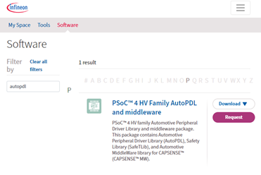
- Go to Infineon Developer Center.
- Under Software, find PSOC™ 4 HV Family AutoPDL and middleware and click on Request to get access to the AutoPDL software.
Once the order request is approved, you will receive an email from Infineon Developer Center (R-IFX-DeveloperCent@infineon.com). Product installer key (License Key) and a link to download the software will be included in the email.
Standard installation procedure
After you download the software and extract the archive, follow the instructions to install AutoPDL.
- AutoPDL Middleware package
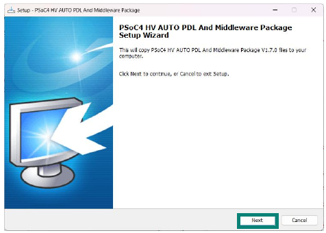
- Run the PSOC4HV_AutoPDL-MW_V1.7.0_BulkInstall.bat in the
\WWxxxx_PSOC4HV_AutoPDL-MW_Vx.x.x
folder. After the setup wizard appears, click Next.
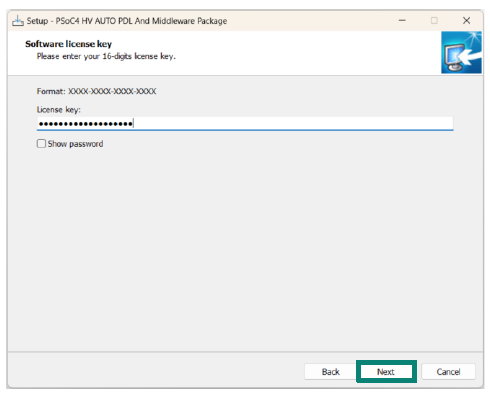
- Enter the License key which is
including in email from Infineon Developer Center and click Next.
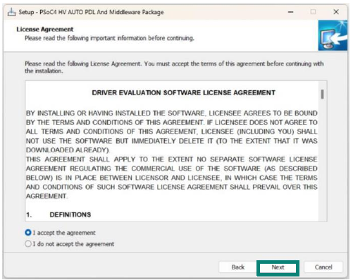
- Read the license agreement. Select I accept the agreement and click
Next.
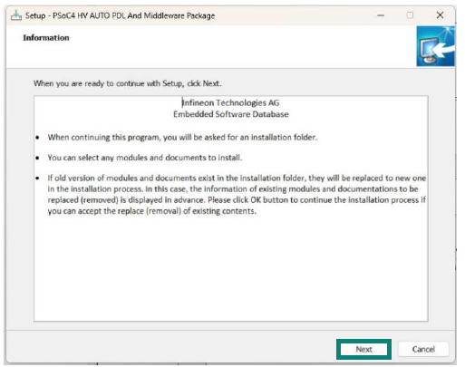
- Read the information and click Next.
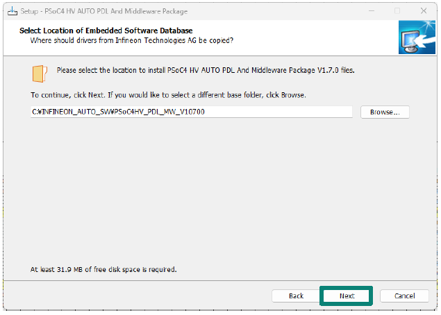
- Select the install folder and click Next to continue.
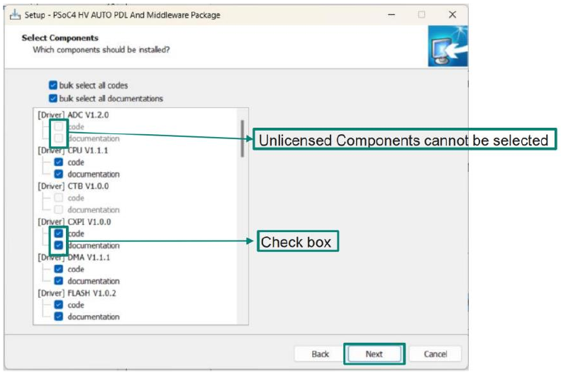
- Select the components that you want to install and click Next to continue.
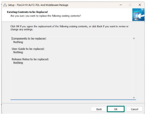
- The Auto PDL and middleware package installer checks for the existing Auto
PDL drivers/middleware and documents in the installation folder. The
existing drivers/middleware and documents are displayed. If you want to
replace the existing contents, click OK.
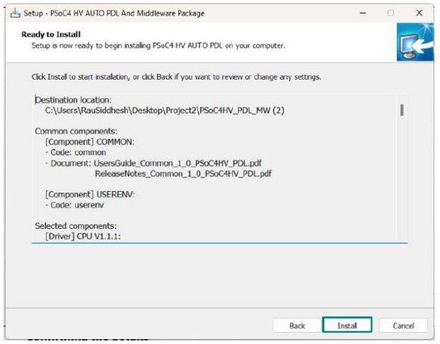
- Confirm the details and click Install.
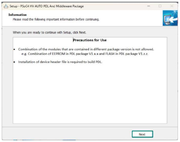
- Read the Precautions for Use and click Next.
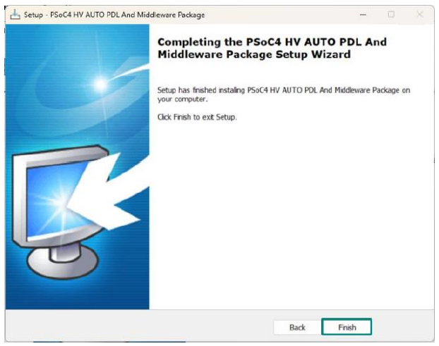
- Click Finish to complete the
installation.
- Run the PSOC4HV_AutoPDL-MW_V1.7.0_BulkInstall.bat in the
\WWxxxx_PSOC4HV_AutoPDL-MW_Vx.x.x
folder. After the setup wizard appears, click Next.
- Device Header Files
- The setup wizard for device header files is automatically appeared.
- In the setup wizard, click Next.
- Read the license agreement. Select I accept the agreement and click Next.
- Read the information and click Next.
- Select the install folder same as selected while installing the Middleware.
Click Next to continue.
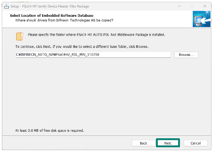
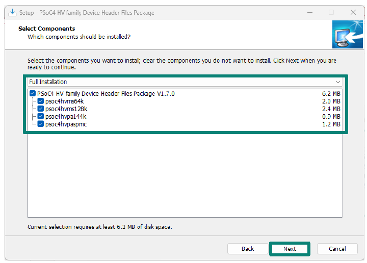
- Select the HV Device for which you want to install headers and click
Next to continue.
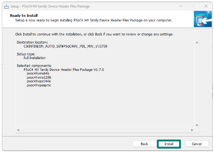
- Check your selection and click on install.
- Click Finish to complete the installation.
- Code Examples
The setup wizard for code examples automatically appear.
- In the setup wizard, click Next.
- Read the license agreement. Select I accept the agreement and click Next.
- Read the information and click Next.
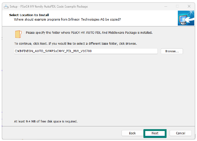
- Select the install folder same as selected while installing the middleware
and device header. Click Next to
continue.
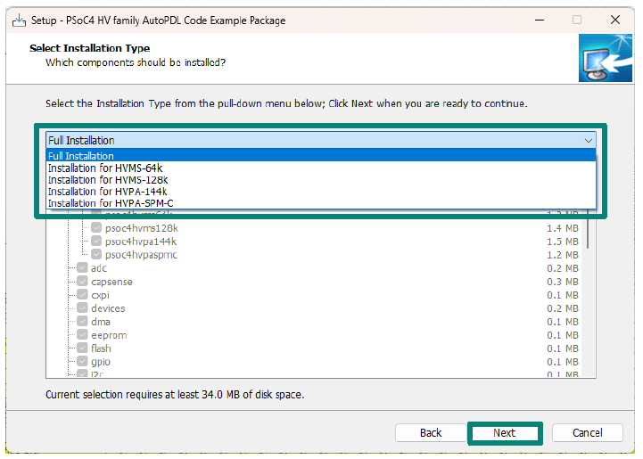
- Select the HV Device for which you want to install code example from the
drop down as shown in the following figure. Click Next to continue.
- Check your selection and click on install.
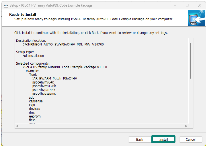
- Click Finish to complete the installation.
IAR EWARM flash patch configuration update
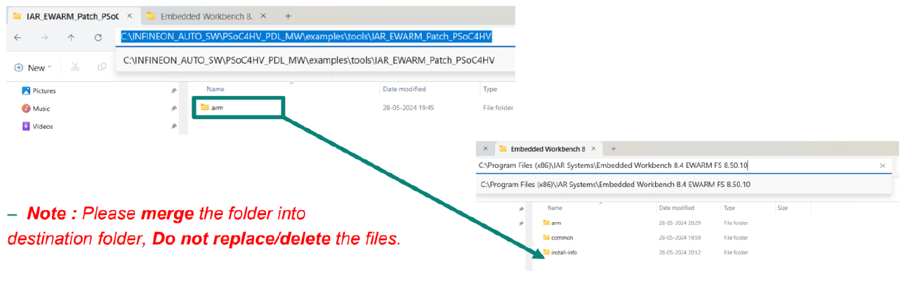
Copy and paste (or replace) the flash loader files (arm folder) to the IAR installation folder.
- Copy from AutoPDL installation:
- C:\INFINEON_AUTO_SW\PSOC4HV_PDL_MW_Vxxxxx\examples\Tools\IAR_EWARM_Patch_PSOC4HV
- Paste (or replace) to IAR installation:
- C:\Program Files (x86)\IAR Systems\Embedded Workbench 8.4 EWARM FS 8.50.10
Example usage of AutoPDL
- Navigate to the AutoPDL folder and open the
PSOC4hvpa144k_Eva_license.eww file.
C:\INFINEON_AUTO_SW\PSOC4HV_PDL_MW_Vxxxxx\examples\Tools\PSOC4hvpa144k
Note: If you use the source code license, open the PSOC4hvpa144k_flash_cm0plus_template.eww.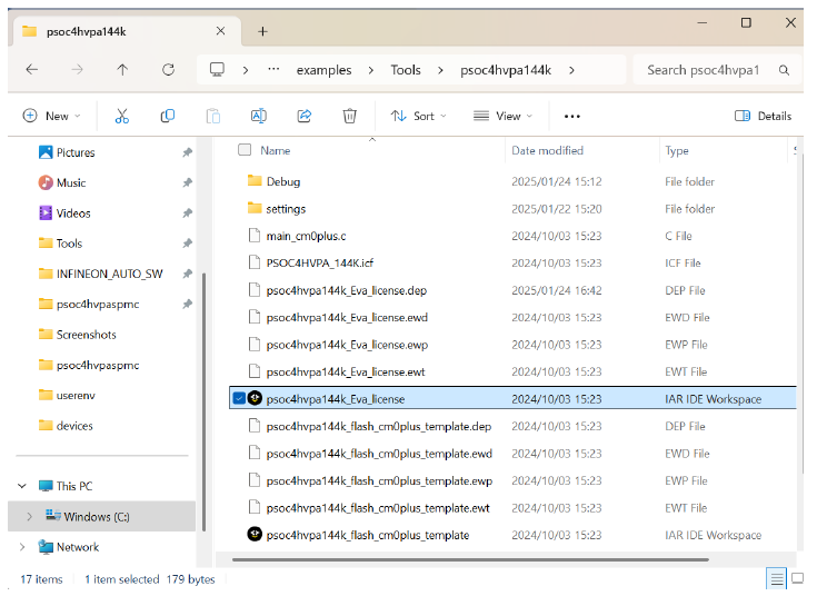
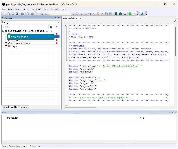
- Double-click on main_cm0plus.c in the left
panel. Details of the sample code are shown (see Code Listing 2).
-
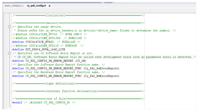
Write the Define value for your target device.
e.g. C:\INFINEON_AUTO_SW\PSOC4HV_PDL_MW\source\userenv\cy_pdl_config.h
The device names supported by the standard evaluation board are as follows:
- HVPA144K: CY8C4147LCE_HV423 (Evaluation board) or CY8C4147LCE_HV413 (Lite-Kit Board)
- HVMS64K: CY8C4146LWE_HVS115
- HVMS128K: CY8C4147LWE_HVS135X
- HVPASPM-C: CY8C4147LDE_HV734
If you are using a Lite-Kit board, please also add the following definitions.
- HVPA144K: KIT_PSOC4_HVPA_144K_LITE
- HVMS128K: KIT_PSOC4_HVMS_128K_LITE
If you are using HVPA-144K_LITE, change it as follows:
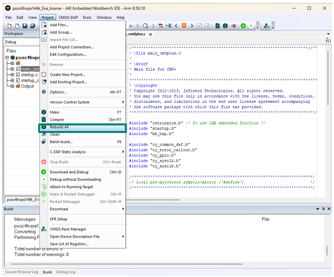
- Select Project > Rebuild
All to build the project.
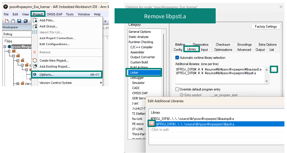
 Note: If you didn’t request a SafeTlib license, two errors will occur. If you see the errors, remove the cy_pstl_user_callout.c and libpstl.a files and then select Rebuild all. To remove the cy_pstl_user_callout.c file, right-click the file and then click Remove. To remove the libpstl.a file, navigate to Project > Options > Linker > Library tab and click the ellipses button next to the Additional libraries pane. Select libpstl.a and click remove (×).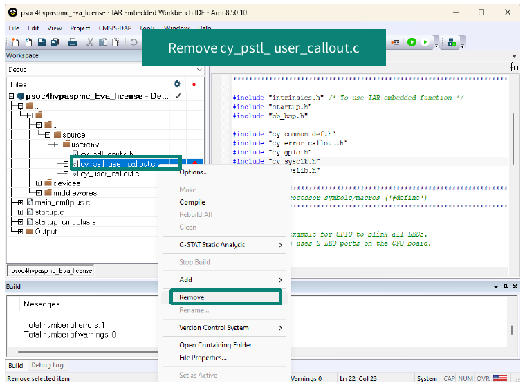
- Connect the USB cable to the J4 and 12V wall Adapter to the J22 of
the CYHVPA-128K-32-001 Evaluation Board with the power supply (See Figure 8). See the PSOC™ HV PA Evaluation Board user guide 3 for more detailed
information.
Figure 8. USB cable connection
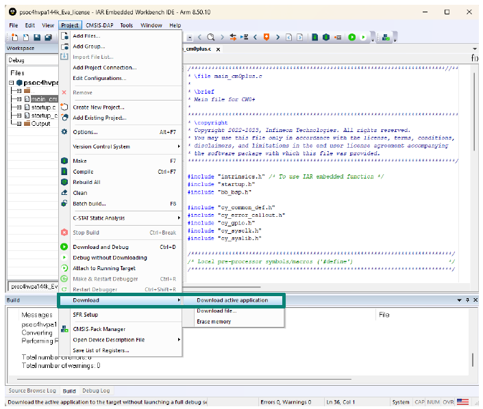
- Download the project to PSOC™ 4 HVPA-144K device by selecting Project >
Download > Download active application.
- Push the reset switch (SW2) on the
CYHVPA-128K-32-001 Evaluation Board and then confirm that the LED D6 and D7 are
blinking.
- Download the application using the IAR I-JET debugger
- Connect the IAR I-jet Debugger to either J3
(MIPI 20-pin) or J5 (MIPI 10-pin) of the CYHVPA-128K-32-001 Evaluation Board with
power supply (See Figure 9). See the PSOC™ HV PA Evaluation Board user guide 4 for more detailed
information.
Figure 9. Connection of IAR I-jet Debugger
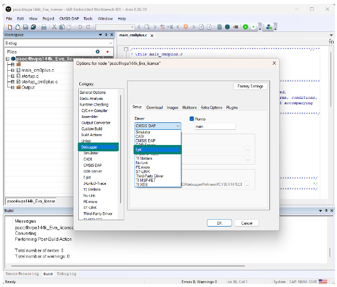
Note: Please check I-jet is set for Debugger. In case of the CMSIS DAP program, the menu name shows CMSIS DAP. If it isn’t, navigate to Project > Options > Debugger and select I-jet at Driver.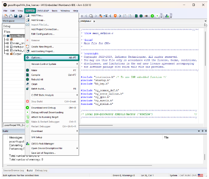
-
- Download the project to PSOC™ HV PA
device by selecting Project >Download > Download active
application.
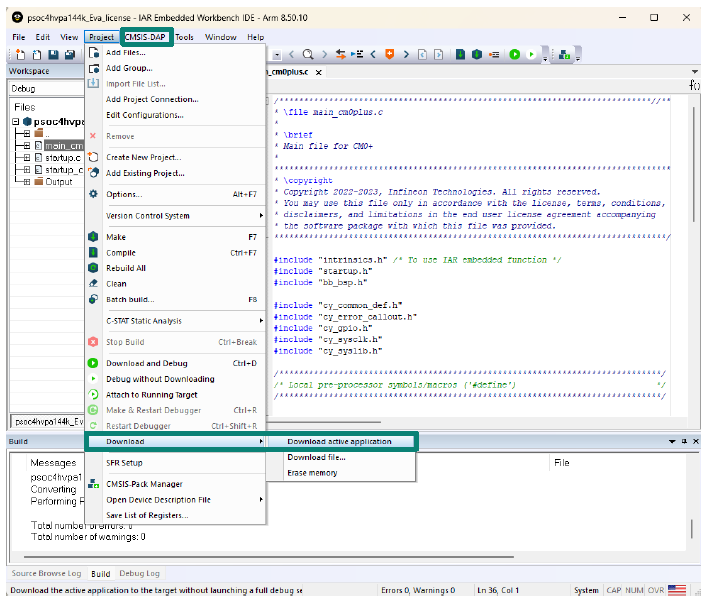
- Download the project to PSOC™ HV PA
device by selecting Project >Download > Download active
application.
-
- Push the reset switch (SW2) on the CYHVPA-128K-32-001 Evaluation Board and
then confirm that the LED D6 and D7 is blinking.
- Download the application using the onboard KitProg3
- Push the reset switch (SW2) on the CYHVPA-128K-32-001 Evaluation Board and
then confirm that the LED D6 and D7 is blinking.
- Connect the USB cable to the J4 of the CYHVPA-128K-32-001 Evaluation
Board with the power supply (See Figure 10).
See the PSOC™ HV PA Evaluation Board user guide
4 for more
detailed information.
Figure 10. USB cable connection
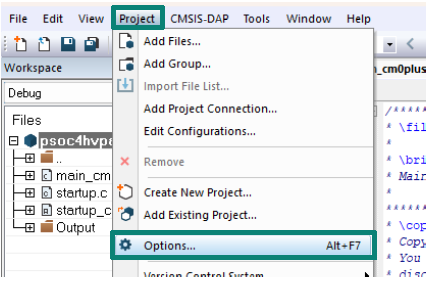
- Select Project > Options… to change the
debugger settings.
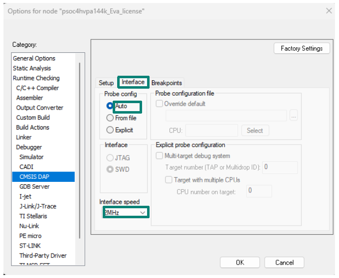
- Select CMSIS DAP from Options and select the
Interface tab. Change the settings as shown in:
- Probe config -> Auto
- Interface speed -> 2MHz
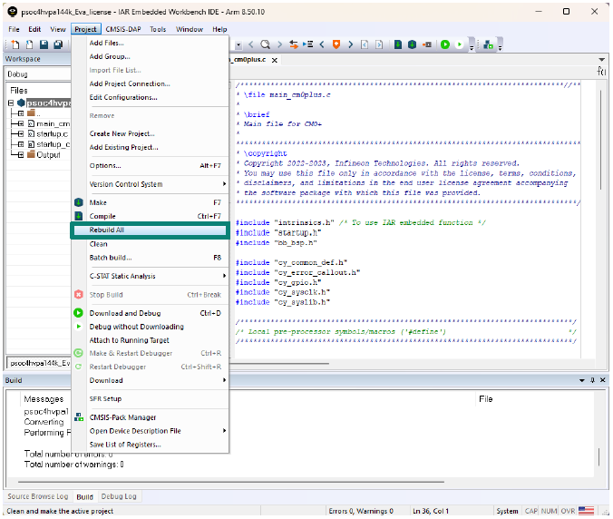
- Click OK and re-select Project >
Rebuild All to build the project.
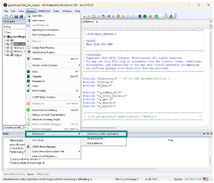
- Download the project to PSOC™ HV PA device by
selecting Project > Download > Download active
application.
Push the reset switch (SW2) on the CYHVPA-128K-32-001 Evaluation Board and then confirm that the LED D6 and D7 is blinking.
To debug the project using either IAR I-JET debugger or onboard KitProg3 (CMSIS DAP), select Project > Download and Debug. For more information on debugging, see the IAR EWARM IDE project management and building guide 5.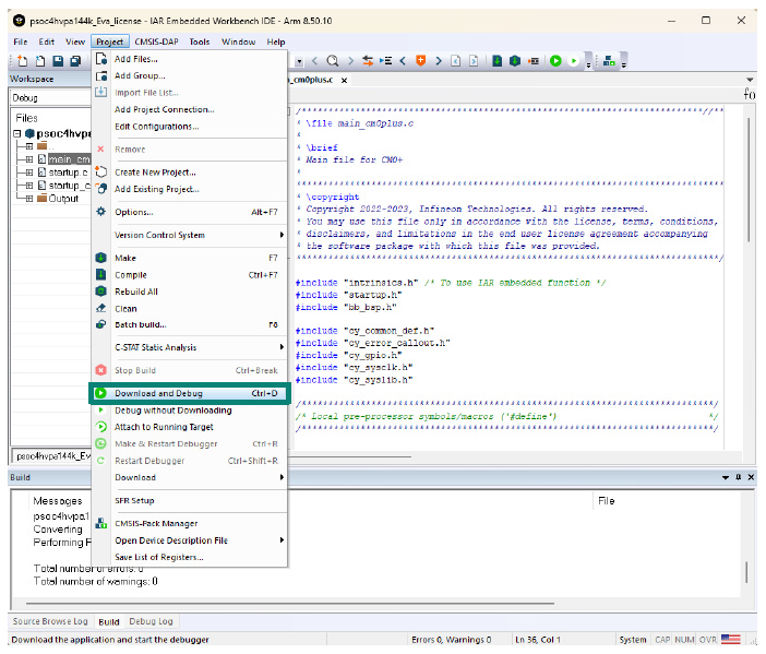
Other sample codes
The other code examples are in the examples folder.
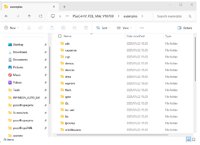
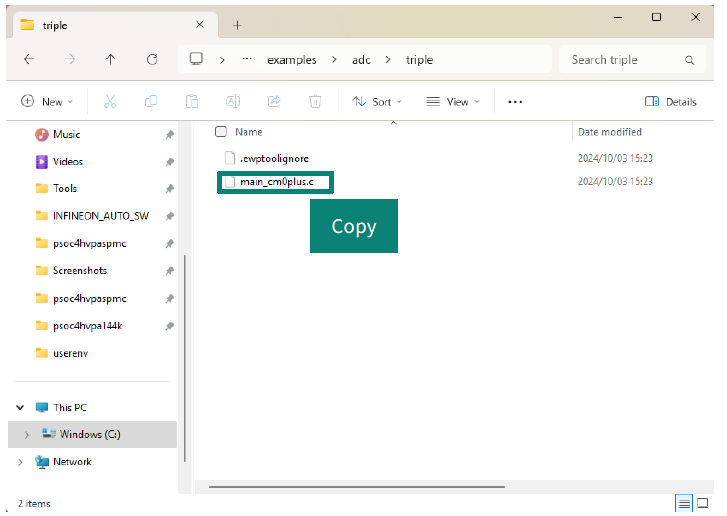
- Go to any code sample folder (e.g., ) and copy the main_cm0plus.c file in
the folder.
- Navigate to
PSOC4HV_PDL_MW_Vxxxxx\examples\Tools\PSOC4hvpa144k and replace
the copied main_cm0plus.c file.
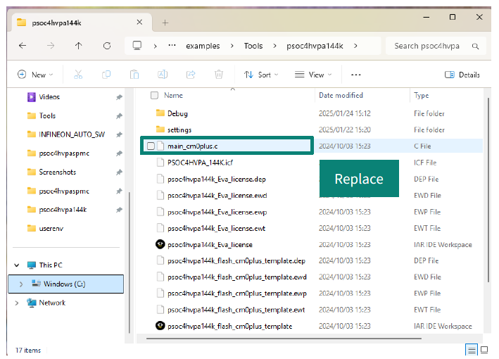
- From the same folder, open PSOC4hvpa144k_Eva_license.eww (or PSOC4hvpa144k_flash_cm0plus_template.eww for source file license) to open the IAR EWARM sample project.
- Rebuild and download the project to the board. See the C:\INFINEON_AUTO_SW\PSOC4HV_PDL_MW_Vxxxxx\examples\readme.pdf file of the sample codes for a detailed explanation of the use case.
Development tools
| Vender | Emulators/probes | Compiler |
|---|---|---|
|
IAR Systems |
I -JET Debugger Onboard KitProg3 |
EWARM (8.50.10) |
Flash programming tools
Table 5 lists the supported flash programming tools. Infineon MiniProg4 programmer is for development purposes. For mass production purposes, a JTAG programmer from a third-party is suitable.
| Vender | Flash programmer | Software |
|---|---|---|
|
Infineon |
MiniProg4 |
Infineon Auto Flash Utility |
|
KitProg3 |
Table 6 lists the pin assignment for Cortex® debug connector.
| Pin | Signal |
|---|---|
|
1 |
VDDD |
|
2 |
SWDIO |
|
3 |
GND |
|
4 |
SWDCLK |
|
5 |
GND |
|
6 |
SWO (option) |
|
7 |
KEY |
|
8 |
NC |
|
9 |
GND detect |
|
10 |
nRESET |
Summary
This application note guided you to set up the PSOC™ HV PA development environment. Infineon provides an evaluation board and a wealth of sample software to help you get started with the PSOC™ HV PA family. To evaluate the CYHVPA-128K-32-001 Evaluation Board, contact your sales representative or Infineon Technical Support.
Glossary
| Terms | Description |
|---|---|
|
A/D converter |
Analog to Digital Converter |
|
ADC |
Analog to Digital Converter |
|
AHB |
Advanced High-Performance Bus |
|
API |
Application Programming Interface |
|
BOD |
Brown-Out Detectors |
|
CM0+ |
Arm® Cortex®-M0+ (processor core name) |
|
CPU |
Central Processing Unit |
|
CPUSS |
CPU Subsystem |
|
DAP |
Debug Access Port |
|
DMA |
Direct Memory Access |
|
DMAC |
DMA Controller |
|
DW |
Data Wire |
|
ECC |
Error Correction Code (safety) |
|
GPIO |
General Purpose I/O |
|
HV |
High-Voltage |
|
I/O |
Input or Output |
|
IAR |
IAR Systems (Company name) |
|
IOSS |
I/O Sub-System |
|
IRC |
Interrupt Controller |
|
IRQ |
Interrupt Request |
|
ISR |
Interrupt Service Routine |
|
LIN |
Local Interconnect Network |
|
MCU |
Microcontroller Unit |
|
MIPI |
Mobile Industry Processor Interface |
|
MPU |
Memory Protection Unit |
|
NMI |
Non-Maskable Interrupt |
|
PA |
Precision Analog |
|
PACSS |
Precision Analog Channel Subsystem |
|
POR |
Power On Reset |
|
PWM |
Pulse Width Modulation |
|
RAM |
Random Access Memory |
|
ROM |
Read-Only Memory |
|
SCB |
Serial Communication Block |
|
SDL |
Sample Driver Library |
|
SPI |
Serial Peripheral Interface |
|
SRAM |
Static RAM |
|
SRSS |
System Resource Subsystem |
|
SWD |
Serial Wire Debugging |
|
TCPWM |
Timer, Counter and PWM |
|
WDT |
Watchdog Timer |
References
The following are the PSOC™ HV PA family series application notes, datasheets, and technical reference manuals. Contact Infineon Technical Support to obtain these documents and sample driver library.
- 002-28660: PSOC™ HV PA-144K datasheet
- 002-29223: PSOC™ HV PA architecture technical reference manual (TRM)
- 002-29238: PSOC™ HV PA registers technical reference manual (TRM)
- 002-29984: PSOC™ HV PA Evaluation Board user guide
- IAR EWARM IDE project management and building guide
- 002-31481: PSOC™ 4 HVPA-144K Safety Manual
Revision history
| Document revision | Date | Description of changes |
|---|---|---|
|
** |
2020-11-24 |
Initial release |
|
*A |
2023-04-07 |
Updated all sections to support the latest silicon |
| *B | 2023-04-19 | Template update; no content update |
| *C | 2025-02-14 | Changed to use AutoPDL. |
Trademarks
PSOC™, formerly known as PSoC™, is a trademark of Infineon Technologies. Any references to PSoC™ in this document or others shall be deemed to refer to PSOC™.