About this document
Scope and purpose
This application note provides guidance on software usage of various SoC peripherals available on CYW20829 along with its use cases.
Intended audience
This document is intended for application developers of AIROC™ CYW20829 who are interested in understanding the features and peripherals of CYW20829.
Overview of CYW20829
Features
- High-performance compute subsystem with Arm® Cortex® M33 core dedicated for rich real-time embedded applications
- Bluetooth® Low Energy (Bluetooth® LE) controller subsystem with Arm® Cortex® M33 with dedicated ROM and RAM for Bluetooth® operations
- CPU subsystem
- 96-MHz Arm® Cortex®-M33 CPU
- ARMv8-M architecture
- Core logic operation at either 1.1 V or 1.0 V
- Datawire (DMA) controller with 16 channels
- 32 KB cache for greater eXecute-In-Place (XIP) performance with low power
- 256 KB SRAM with power and data retention control
- 64 KB ROM
- Bluetooth® subsystem
- 48 MHz Arm® Cortex® M33
- 2.4 GHz RF transceiver with 50 Ω antenna drive
- Configurable TX power for 0 dBm and 10 dBm
- Excellent receiver sensitivity
- LE-1 Mbps: –98 dBm
- LE-2 Mbps: –95 dBm
- Coded PHY 500 kbps (LE-LR): –101 dBm
- Coded PHY 125 kbps (LE-LR): –106 dBm
- Received signal strength indication (RSSI) with 1-dB resolution
- Link layer engine supports up to 16 connections simultaneously, four are peripheral
Block diagram
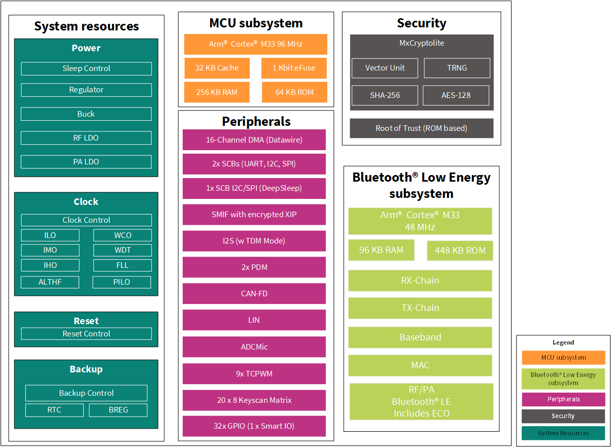
Figure 1 shows the architectural view of CYW20829.
Software architecture
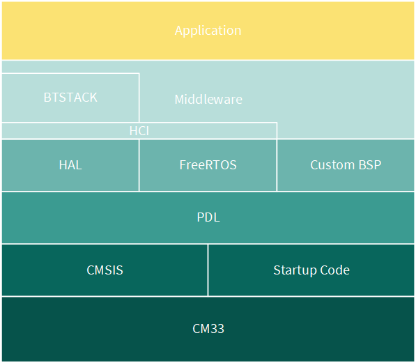
Figure 2 shows the software stack architecture of the CYW20829 CPU subsystem.
Peripheral management
Memory
The CYW20829 follows the Arm® Cortex® M33 compatible memory design architecture. The on-chip memory is isolated across the CPU subsystem and Bluetooth® subsystem. The CPU subsystem consists of 256 KB of RAM, 32 KB of Cache. The Bluetooth® subsystem consists of 448 KB of ROM and 96 B of RAM. The access to Bluetooth® subsystem memory and 64 KB BootROM memory is restricted to user application. The user application will be loaded to external memory such as serial flash or EEPROM and the code will be executed in place. Apart from the application code, some regions of the memory range are occupied for memory mapped on-chip SoC peripherals. These regions of the SoC peripheral memory are readable, writable, non-executable, volatile, and uninitialized at power-up.
Typical memory sections of a program
By default, all the sections of the program memory (serial flash) have the following attributes:
- Readable
- Nonvolatile
| Section | Start address | End address | Length | Write | Execute | Initialized |
|---|---|---|---|---|---|---|
| .appText | 0x08002600 | 0x0800a857 | 0x8258 | FALSE | TRUE | TRUE |
| .copy.table | 0x0800a858 | 0x0800a86f | 0x18 | TRUE | FALSE | TRUE |
| .ARM.exidx | 0x0800a870 | 0x0800a877 | 0x8 | FALSE | FALSE | TRUE |
| .zero.table | 0x0800a878 | 0x0800a87f | 0x8 | TRUE | FALSE | TRUE |
| segment_1 | 0x20000000 | 0x20000113 | 0x114 | TRUE | FALSE | TRUE |
| .ramVectors | 0x20001000 | 0x20001157 | 0x158 | TRUE | FALSE | FALSE |
| .appTextRam | 0x20001158 | 0x20003a6f | 0x2918 | FALSE | TRUE | TRUE |
| .data | 0x20003a70 | 0x20004037 | 0x5c8 | TRUE | FALSE | TRUE |
| .noinit | 0x20004038 | 0x200040af | 0x78 | TRUE | FALSE | FALSE |
| .bss | 0x200040b0 | 0x2002b833 | 0x27784 | TRUE | FALSE | FALSE |
| .heap | 0x2002b834 | 0x2003dbff | 0x123cc | TRUE | FALSE | FALSE |
| .bootstrapText | 0x2003dc00 | 0x2003f5df | 0x19e0 | FALSE | TRUE | TRUE |
| .bootstrapzero.table | 0x2003f5e0 | 0x2003f5e7 | 0x8 | TRUE | FALSE | TRUE |
| .bootstrapData | 0x2003f5e8 | 0x2003f603 | 0x1c | FALSE | FALSE | TRUE |
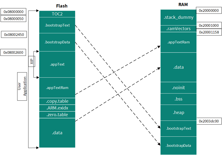
Table 1 shows the typical sections of the application code. Some sections of the program will be copied from an external memory to the RAM, as show in Figure 3.
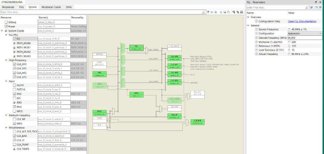
Clock tree
CYW20829 provides flexible clocking options with on-chip crystal oscillators, a frequency lock loop, and support for multiple external clock sources. The CYW20829 device clock system provides clocks to the subsystems that require them, and it allows switching between different clock sources.
Features
- Internal main oscillator (IMO) at a fixed 8 MHz frequency
- Internal high-speed oscillator (IHO) at a fixed 48 MHz frequency
- Precision internal low-speed oscillator (PILO) at a fixed 32.768 kHz frequency
- Internal low-speed oscillator (ILO) at a fixed 32.768 kHz frequency
- Frequency-locked loop (FLL) for logic clocking up to 96 MHz
- Medium frequency oscillator (MFO) at a fixed 2 MHz frequency
- Additional high-frequency clocks can be generated by division
- PERI - Provides the peripheral support
- Watch crystal oscillator (WCO) that requires external crystal with 32.768 kHz frequency
- Enables the configurable clock
- Configurable clock frequency and divider
- Configurable clock sources
Description
Internal main oscillator (IMO)
The IMO is the primary source of internal clocking. It is trimmed during testing to achieve the specified accuracy. The IMO default frequency is 8 MHz, and tolerance is ±2%. The IMO output can be used by the PLL or FLL to generate a wide range of high-frequency clocks, or it can be used directly by the high-frequency root clocks.
Internal low-speed oscillator (ILO)
The ILO operates with no external components and outputs a stable clock at 32.768 kHz nominal. The ILO is a very low-power oscillator, nominally 32 kHz, that operates in all power modes. The ILO can be calibrated against a high-accuracy clock for better accuracy. The ILO is always the source of the watchdog timer (WDT); therefore, enabling the WDT will automatically enable the ILO.
Precision ILO (PILO)
PILO is an additional source that has better frequency stability than ILO. It is intended to replace a watch crystal in Bluetooth® LE products while supporting delay counters that are accurate enough to meet Bluetooth® LE requirements. PILO works in Hibernate and higher modes. PILO can be configured to continue operating during XRES for RTC.
Frequency-locked loop (FLL)
CYW20829 contains one frequency-locked loop (FLL) that resides on clock path 0. The FLL is capable of generating a clock output in the range of 24 MHz to 96 MHz; the input frequency must be between 0.040 Hz and 96 MHz and must be at least 2.5 times less than the CCO frequency. This makes it possible to use the IMO to generate much higher clock frequencies for the rest of the system.
Medium frequency oscillator (MFO)
There is no actual circuit for MFO and it is generated internally by dividing IMO by 4 to generate 2 MHz clock.
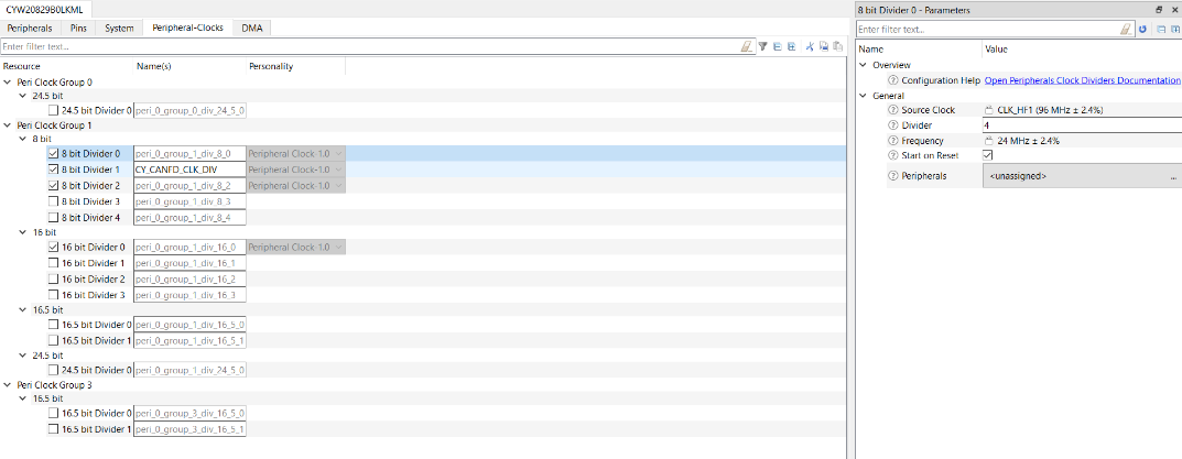
Peripheral clock dividers (PERI)
There are multiple peripheral clock dividers that, in effect, create multiple separate peripheral clocks. The 8-bit and 16-bit dividers are integer dividers. A divider value of ‘1’ means the output frequency matches the input frequency (that is, there is no change). Otherwise, the frequency is divided by the value of the divider. For example, if the input frequency is 50 MHz and the divider is set to ‘10’, the output frequency is 5 MHz. The five fractional bits support further precision in 1/32nd increments. For example, a divider with an integer value of 3 and a fractional value of 4 (4/32) results in a divider of 3.125. Fractional dividers are useful when a high-precision clock is required, for example, for a UART/SPI serial interface. Integer and fractional clock dividers are provided for peripheral use and timing purposes. There are one or more:
- 8-bit clock dividers
- 16-bit integer clock dividers
- 16.5-bit fractional clock dividers
- 24.5-bit fractional clock divider
Internal high-speed oscillator (IHO)
The IHO operates with no external components and outputs a stable clock at 48 MHz.
Clock tree
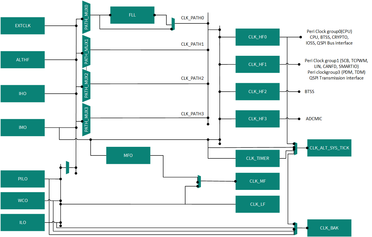
- CLK_HF’s are the Active mode clocks and it can use any clock source from the following clock sources IMO, IHO, ALTHF, and EXTCLK
- CLK_LF is a Deep Sleep domain clock and CLK_BAK is a Hibernate clock and both can select clock sources are from ILO, WCO, and PILO
- IMO is also available in Deep Sleep
Software usage
This section describes the software usage of clock trees using PDL APIs and device configurators. For more information, see the clock PDL APIs in clock tree PDL.
Sequence diagram
- Enable high-frequency clocks (HF1)
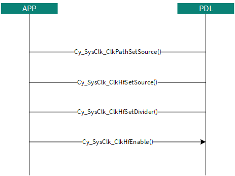
See the following code block to enable HF1 by using Path 1:
/* set the Source of PATH MUX 1 as IMO */
    Cy_SysClk_ClkPathSetSource(1U, CY_SYSCLK_CLKPATH_IN_IMO);
/* Set Source of HF Clock as Clk path mux 1 */
    Cy_SysClk_ClkHfSetSource(1U, CY_SYSCLK_CLKHF_IN_CLKPATH1);
/*Set the Divider to get the Desired HF frequency */
    Cy_SysClk_ClkHfSetDivider(1U, CY_SYSCLK_CLKHF_NO_DIVIDE);
/* Enable Hf1 Clock */
    Cy_SysClk_ClkHfEnable(1U);
- Enable HF3 by changing the source of Clk path mux 1 as IHO
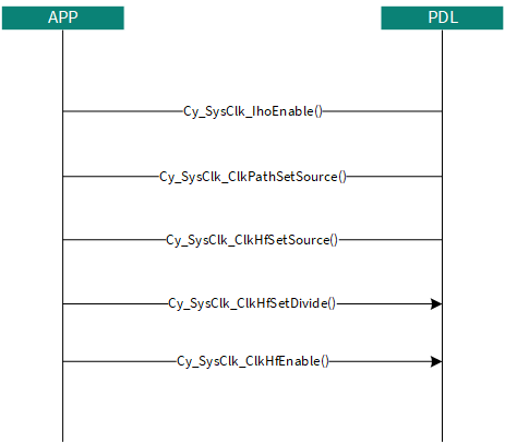
See the following code block to enable HF3 with the source clock path of IHO:
if(!Cy_SysClk_IhoIsEnabled)
    {
    /* Enable IHO */
     Cy_SysClk_IhoEnable()
    }
    /* set the Source of PATH MUX 1 as IMO */
    Cy_SysClk_ClkPathSetSource(1U, CY_SYSCLK_CLKPATH_IN_IHO);
    /* Set Source of HF Clock as Clk path mux 1 */
    Cy_SysClk_ClkHfSetSource(3U,  CY_SYSCLK_CLKHF_IN_CLKPATH1);
    /*Set the Divider to get the Desired HF frequency */
    Cy_SysClk_ClkHfSetDivider(3U, CY_SYSCLK_CLKHF_NO_DIVIDE);
    /* Enable Hf1 Clock */
    Cy_SysClk_ClkHfEnable(3U);
- Configuring the peripheral clock for SCB
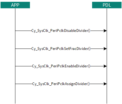
See the following code block to configure the peripheral clock for SCB:
Cy_SysClk_PeriPclkDisableDivider(PCLK_SCB2_CLOCK_SCB_EN, CY_SYSCLK_DIV_16_5_BIT, 0U);
   /* Sets one of programmable divider for SCB2 */
   Cy_SysClk_PeriPclkSetFracDivider(PCLK_SCB2_CLOCK_SCB_EN, CY_SYSCLK_DIV_16_5_BIT, U, 12U, 10);
   /* Enable the Selected Divider  rrfrrrr */
   Cy_SysClk_PeriPclkEnableDivider(PCLK_SCB2_CLOCK_SCB_EN,  CY_SYSCLK_DIV_16_5_BIT, 0U);
   /* Assigns the Divider to SCB2 block  */
   Cy_SysClk_PeriPclkAssignDivider(PCLK_SCB2_CLOCK_SCB_EN, CY_SYSCLK_DIV_16_5_BIT, 0U);
Device Configurator
The device configurator in ModusToolbox™ lets you choose various clock sections and their parameters as well. Additionally, you can use HAL APIs to configure basic clock parameters.
Applications and code examples
Clock tree use cases are:
- System clock (systick)
- Periodic functions (Callbacks)
- Simple timer
For example, see CYW20829 clock frequency measurement, which demonstrates how a clock measurement counter can be used to measure the internal clock signal using another clock signal as a reference. Here, the IMO clock is used as a reference clock to measure internal clock signals such as the internal high-frequency clocks HFO, HF1, HF2, and HF3.
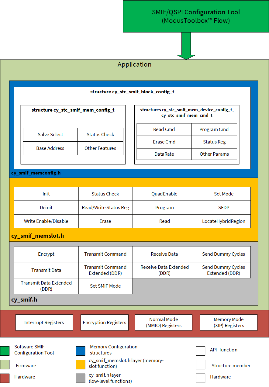
Serial memory interface (SMIF)
SMIF is designed to provide a convenient and efficient means of communicating with serial flash memories, enabling the CYW20829 SoC to read, write, and erase data from the memories. By using the SMIF interface, developers can easily integrate serial flash memories into their applications, allowing for more versatile and scalable memory solutions. The SMIF in CYW20829 is an IP for external serial connectivity that provides high-performance communication to the external memories. The SPI-based communication interface to the external quad SPI (QSPI) high-speed memory devices.
Features
- Supports eXecute-In-Place (XIP) from external quad flash
- Supports DDR
- Supports for single, dual and quad interfaces with throughput up to 384 -Mbps
- XIP mode also supports AES-128 based on-the-fly encryption and decryption, enabling secure storage and access of code and data in the external memory
Description
The SMIF IP block implements a SPI-based communication interface for interfacing external memory devices to CYW20829. The SMIF supports SPI, dual SPI (DSPI), and quad SPI (QSPI) configurations. The primary usage model for the SMIF is that of an external memory interface, and it operates at a maximum frequency of 48 MHz.
The MMIO mode is used for implementing a generic SPI/DSPI/QSPI/communication interface using the SMIF block. This interface can be used to implement special commands such as program or erase of flash, memory device configuration, sleep mode entry for memory devices, or other special commands specific to the memory device. The transfer width (SPI, DSPI, or QSPI) of a transmission is a parameter set for each transmit and receive operation. Therefore, these can be changed at run time. In a typical memory interface with flash memory, the SMIF is used in the memory mode while reading from the memory, and it switches to the normal mode when writing to flash memory. A typical memory device has multiple types of commands. The SMIF interface can be used to transmit different types of commands.
XIP is a mode of operation where read or write commands to the memory device are directed through the SMIF without any use of API function calls. In this mode, the SMIF block maps the AHB bus accesses to external memory device addresses to make it behave like internal memory. This allows the CPU to execute code directly from external memory.
XIP mode is not limited to code and is suitable for data read and write
accesses. The memory regions available for XIP address allocation are defined in a
linker script file (.ld). The XIP interface is protected by MPC
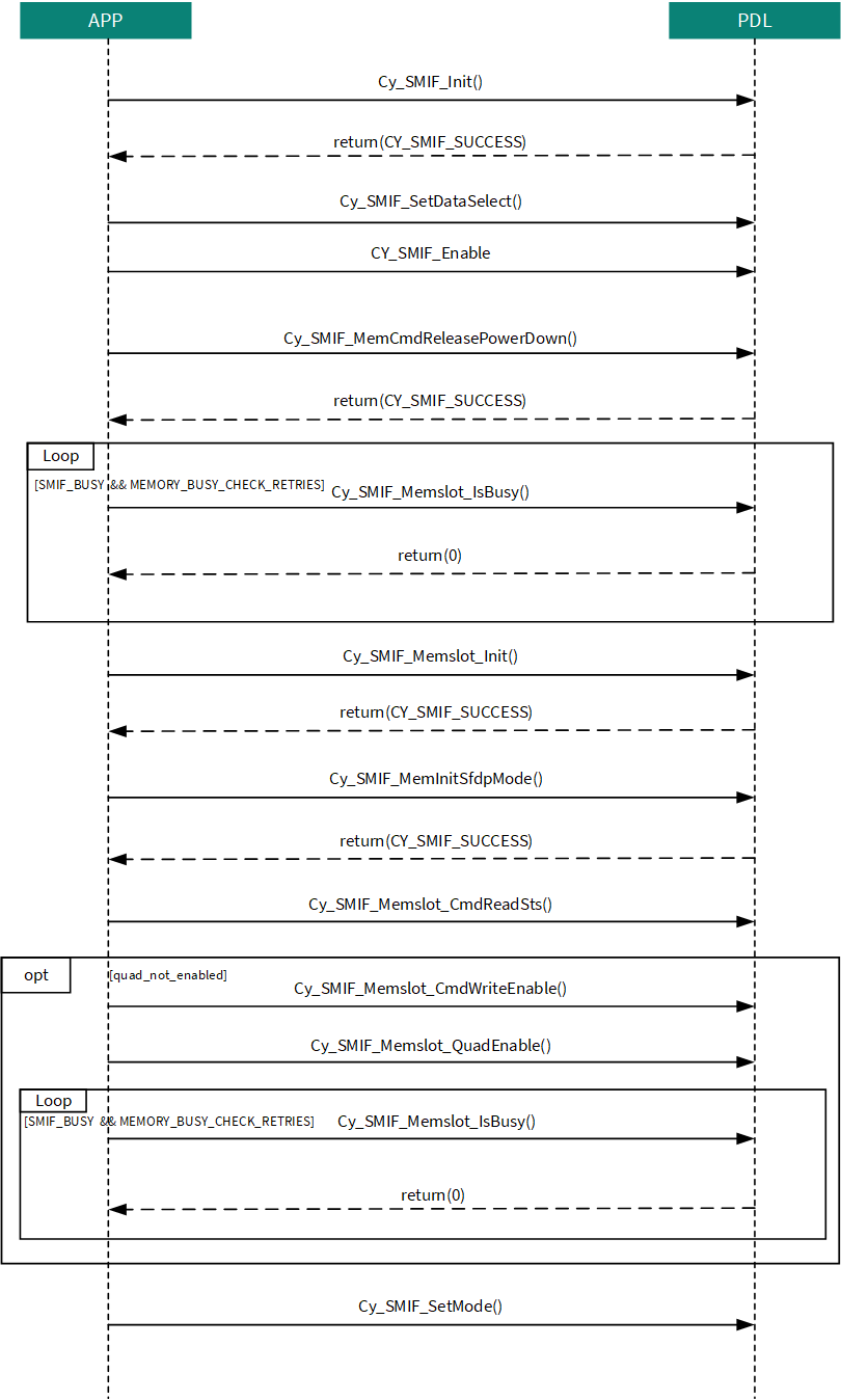
integrated into SMIF, along with associated interrupts and MMIO. Figure 12
shows the SMIF sequence diagram. Call the
cybsp_smif_init() API to initialize the SMIF. Use the
Cy_SMIF_MemCmdReleasePowerDown() API to send the
release power-down command, and then use the
Cy_SMIF_Memslot_IsBusy() API to check if the status of
the device is busy.
Block diagram
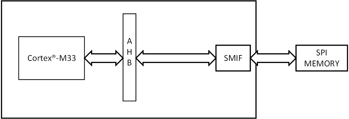
The SMIF provides the interface between the Cortex®-M33 and the external memory device via AHB.
The SMIF block maps the AHB bus accesses to external memory device addresses to make it behave like internal memory. This allows the CPU to execute code directly from external memory.
| Memory device | IO signals |
|---|---|
| Single SPI memory | SCK, CS, SI, and SO. This memory device has two data signals (SI and SO) |
| Dual SPI memory | SCK, CS, IO0, and IO1. This memory device has two data signals (IO0, IO1) |
| Quad SPI memory | SCK, CS, IO0, IO1, IO2, and IO3. This memory device has four data signals (IO0, IO1, IO2, and IO3) |
Software usage
Sequence diagram
Device Configurator
Do the following to initialize the SMIF:
- Open the Device Configurator. Navigate to the Peripheral tab in the Device Configurator
- Select the checkbox next to the QSPI option
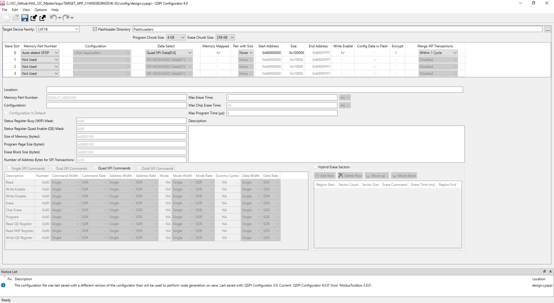
This generates the initialization code. On the right side of the Device Configurator window, you can configure the Interface Clock, SPI Clock, and Data Lines for the SMIF. Additionally, the Device Configurator provides a Code Preview window that displays the defines and functions related to the QSPI configuration.
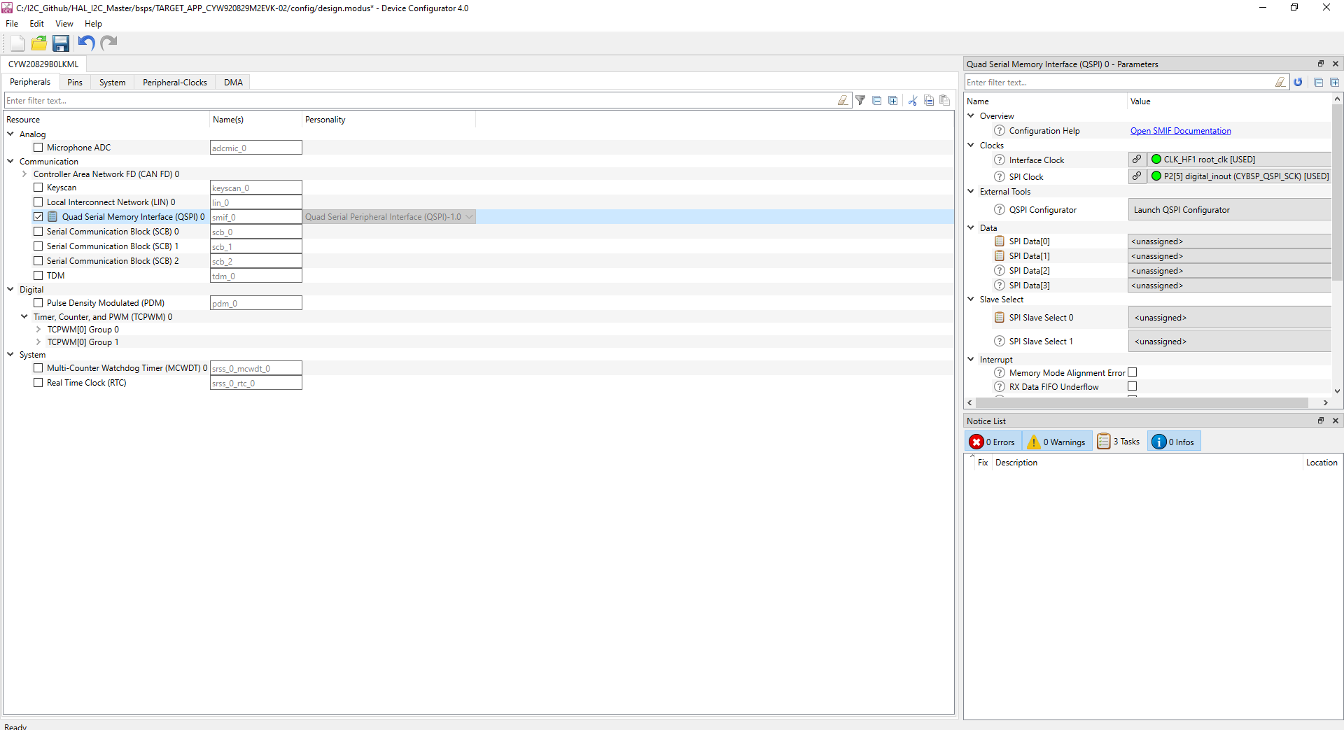
Additionally, the QSPI configurator provides the flexibility to initialize the QSPI memory configuration. You can select the Memory Part number, Data Select, enable and disable the encryption, and so on.
Applications and code example
SMIF use cases are:
- To interface an external flash to the SoC
- To perform XIP (“on-the-fly” translation of read and write transfers on the XIP AHB interface to external memory SPI transfers)
For example, see the following:
- Serial flash read and write, which demonstrates interfacing an external NOR flash memory and performing read and write operations using the serial flash library
- Code example: Demonstrates how to initialize the SMIF for XIP
GPIO
GPIO is a term used to describe a collection of pins or ports that can be found on various electronic devices, including microcontrollers, single-board computers, and embedded systems. These pins are specifically designed to offer a flexible interface for connecting and managing external devices or circuits. The GPIO pins can be configured to serve as either input or output channels, granting the device the ability to receive information from external sensors or transmit signals to control other components. When functioning as input pins, they have the capability to detect the state or voltage level of an external signal. Conversely, when operating as output pins, they can generate or produce signals with varying voltage levels. The number of GPIO pins available on a device may vary depending on the specific hardware being used. Typically, each pin is assigned a unique number or identifier, which is utilized for programmatic interaction. Developers have the ability to write software code that can read the state of input pins or set the state of output pins, enabling them to establish connections with a wide range of external components, such as buttons, sensors, LEDs, and more. The GPIO interface offers a versatile means of communication and control between a device and its external environment.
Features
- Separate Set, Clear, and Invert Registers for output
- Interrupt configurations on all GPIO pins, edge-triggered on rising, falling, or both edges
- Frozen mode for latching current state
- Overvoltage tolerant pins (OVT_GPIO)
- Eight drive modes including pull-up/down, open drain drive HIGH and LOW
- Slew rate control to control speed for each GPIO
- Automatic place and route of signals to and from GPIOs
- Analog and digital input and output capability
Description
The configuration information for I/O cells in the GPIO component is communicated through registers. In the power mode of System Deep Sleep, these registers are preserved, while in the Hibernate power mode, they are reset to their default values. In order to enable the Hibernate Interrupt feature, the configuration information of the I/O cells is preserved or frozen when transitioning into System Deep Sleep or Hibernate power modes. Consequently, the configuration signals can be directed within the system's HP (high power), LP (low power), or ULP (ultra-low power) modes.
The configuration of I/O cells encompasses various details, such as the drive mode (pull-up/pull-down) and drive strength. This configuration information may be specific to individual I/O pads, including details like drive mode, drive strength, slew control transitioning (fast or slow), input buffer mode, and more. Through the I/O port, software can access the I/Os to write output signals and read input signals. By leveraging these capabilities, software can carry out bit-banging operations. The signals for GPIO data input, data output, and data output enable in I/O cells are connected via the HSIOM functional connections. The HSIOM register fields determine the specific connection.
Block diagram
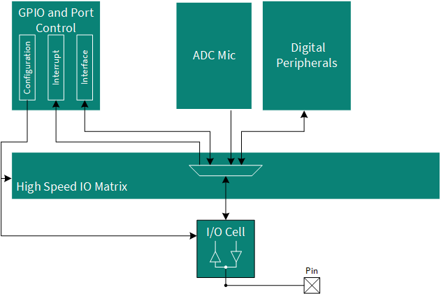
The GPIO pins establish a connection with I/O cells, which are equipped with an input buffer to facilitate digital input with high input impedance as well as a driver for digital output signals. The I/O cells are linked to digital peripherals through the high-speed I/O matrix (HSIOM). Each pin's HSIOM incorporates multiplexers that establish a connection between the chosen peripheral and the pin.
Software usage
This section describes about the software usage of GPIO using PDL and HAL APIs and device configurator. For more documentation, see the GPIO HAL APIs and PDL APIs in the following:
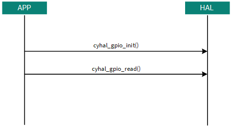
Sequence diagram
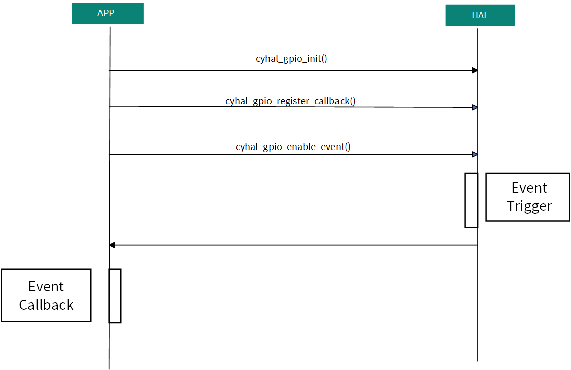
Device Configurator
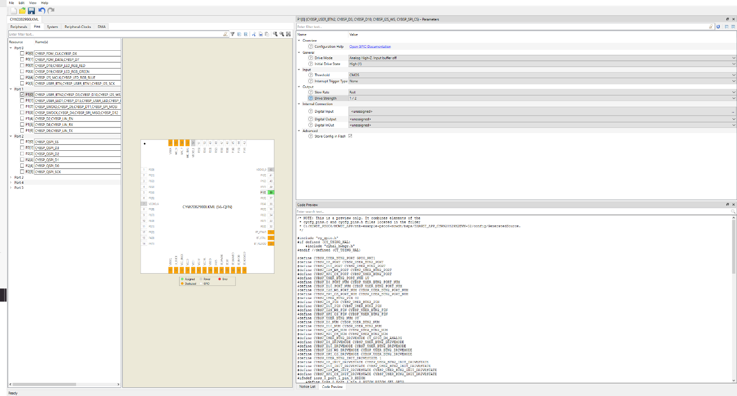
Do the following to initialize the GPIO:
- Use the following methods to access the Device Configurator:
- Right-click on the project and select ModusToolbox™, and then select Device Configurator
Or
- Click Device Configurator in the bottom left corner of the Quick Panel of ModusToolbox™
- Navigate to the Peripheral tab in the Device Configurator
- Select the checkbox in the Pins section
This action generates the initialization code. On the right side of the Device Configuration window, you can configure parameters such as Drive Mode, Initial Drive State, Interrupt Trigger Type, Slew Rate, and Drive Strength
- Go to File and click Save before closing the Device Configurator. Additionally, the Device Configurator provides a Code Preview window that displays the defines and functions related to the GPIO configuration
Applications and code example
GPIO use cases are:
- LED Blinking with GPIO and Delay
- LED Breathing using TCPWM
For example, HAL: GPIO interrupt demonstrates the use of a GPIO configured as an input pin to generate interrupts on an Infineon MCU. The GPIO signal interrupts the CPU and executes a user-defined interrupt service routine (ISR). The GPIO interrupt acts as a wakeup source to wake the CPU from Deep Sleep.
Serial Communication Block (SCB)
The SCB has the capability to support three different serial communication protocols, such as SPI, UART, and I2C. However, note the following:
- A SCB can support only one of these protocols at any given time
- Not all SCBs are capable of supporting all three modes (SPI, UART, and I2C)
- Not all SCBs operate in Deep Sleep mode. To determine which SCBs operate in Deep Sleep and which SCB is capable of supporting which mode, see the device datasheet for specific information
Features
- Standard I2C master and slave functionality
- Trigger outputs for connection to DMA
- Each SCB has a 256-byte FIFO for receive (Rx) and transmit (Tx)
- Multiple interrupt sources to indicate status of FIFOs and transfers
- Local loop-back control
- Deep Sleep-capable SCB features:
- EZ mode for SPI and I2C slaves , allows for operation without CPU intervention
- CMD_RESP mode for SPI and I2C slaves ,allows for operation without CPU intervention
- Low-power (Deep Sleep) mode of operation for SPI and I2C slaves (using external clocking)
- Deep Sleep wakeup on I2C slave address match or SPI slave selection
Description
Every SCB is equipped with 256-byte dedicated RAM specifically designed for transmit and receive operations. This RAM can be configured in three distinct modes: FIFO mode, EZ mode, and Command-Response mode. Masters can only use FIFO mode. UART only uses FIFO mode. I2C and SPI slaves can use all three modes.
EZ and CMD Response modes are available only on the Deep Sleep-capable SCB.
The SCB can receive clock signals from two sources: either an internal clock provided by the peripheral clock dividers or an external master clock. However, for UART, SPI master, and I2C master modes, the SCB must use clk_scb as the clock source. SPI slave and I2C slave modes can utilize the clock from an external master; however, this capability is limited to the Deep Sleep-capable SCBs.
SPI
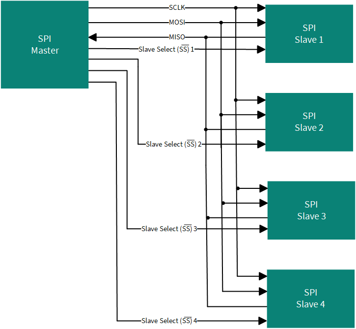
The SPI protocol is a synchronous serial interface protocol that allows devices to function in either master or slave mode. Data transfer initiation is the responsibility of the master device. The SCB facilitates a single-master-multiple-slaves topology for SPI communications, with multiple slaves being supported and having their individual slaves select lines. During the SPI data transfer, the master selects a slave by asserting its SS line, and subsequently, it transmits data on the MOSI line along with a clock signal on the SCLK line. Depending on the configuration, the slave captures data on the MOSI line using either the rising or falling edges of the SCLK signal while simultaneously sending data on the MISO line, which is then captured by the master. This block supports the following features.
- Support both master and slave functionality
- Activating wake-up interrupt cause upon slave selection
- Offering three modes: FIFO mode, EZ mode (for slaves only), and CMD_RESP mode (for slaves only)
- Local loop-back control
- Support interrupts or a polling CPU interface for data handling
Block diagram
A SPI interface has the following four signals:
- SCLK: Clock output from the master, input to the slave
- MOSI: Data output from the master, input to the slave
- MISO: Data input to the master, output from the slave
- Slave Select (SS): Output from the master, input to the slave
UART
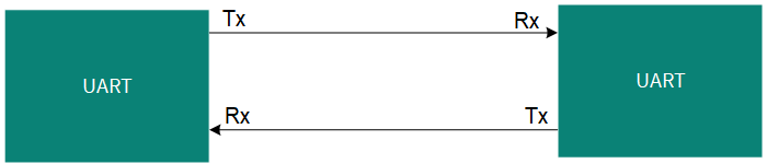
The UART protocol is an asynchronous serial interface used for point-to-point communication. TX (Transmitter output) and RX (Receiver input) are the two main signals. For flow control in UART, the following two additional side-band signals are utilized; however, note that the flow control applies only to the TX functionality.
- Clear to Send (CTS), an input signal to the transmitter, indicating that the receiver is ready to receive data, allowing the transmitter to send the data
- Request to Send (RTS), an output signal from the receiver, which becomes active when the receiver is ready to receive data. The RTS of one device is connected to the CTS of the other device and vice versa. Therefore, when a device (receiver) is prepared to receive data, it activates its RTS, triggering the CTS of the other device (transmitter), signaling it to send the data
This block supports the following features:
- Data frame size programmable from 4 to 9 bits
- Programmable amount of STOP bits
- Parity support (odd and even parity)
- Transmitter and receiver functionality
- Start skipping
- Hardware flow control
Block diagram
The UART transfer is initiated with a start bit, followed by several data bits, and optionally a parity bit, concluding with one or more stop bits. The start and stop bits serve to mark the beginning and end of data transmission. The transmitter includes the parity bit, which allows the receiver to identify single-bit errors. Due to the asynchronous nature of the interface, there is no shared clock between the transmitter and receiver. Therefore, both parties must synchronize and settle on the same baud rate for effective communication.
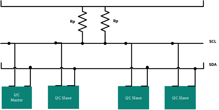
I2C
Every SCB supports both I2C master and slave modes. However, only SCB[0] is accessible in system Deep Sleep power mode and permits externally-clocked operations. This section describes the software usage of SCB using PDL and HAL APIs and a device configurator. I2C is an asynchronous serial interface that supports single-master, multi-master, and multi-slave configurations. Devices can function as either a master, slave, or master/slave. In master/slave mode, a device switches between master and slave roles depending on the address it receives. During a data transfer, only one master can be active at a time, and this active master is responsible for generating the clock signal on the SCL line. This block supports the following features:
- Master, slave, and master-slave functionality
- Clock stretching
- Multi-master modes and bus arbitration
- Programmable oversampling of I2C clock signal (SCL)
- Wake up from sleep modes
Block diagram
The standard I2C bus consists of two wires, namely Serial Data (SDA) and Serial Clock (SCL). I2C devices utilize open collector or open-drain output stages and are connected to these lines along with pull-up resistors (Rp). Devices in the I2C bus have a straightforward master/slave relationship, and they can function as either transmitters or receivers. Each slave device on the bus is uniquely addressable by a 7-bit address through software.
Software usage
This section describes the software usage of SCB (SPI, UART, and I2C) using PDL and HAL APIs and a device configurator. For more details on SCB (SPI, UART, and I2C) HAL APIs and PDL APIs, see the following:
Sequence diagram
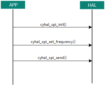
Use case 1: Configuration to send command packets by SPI master.
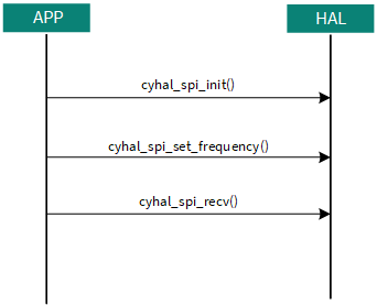
Use case 2: Configuration to receive command packets by SPI slave.
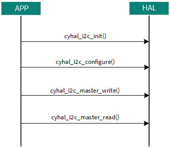
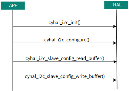
Use case 3: Configuration to read and write by I2C master.
Use case 4: Configuration to read and write by I2C slave.
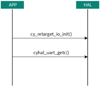
Use case 5: Simple UART communication to read.
Device Configurator
Do the following to initialize the SCB:
- Use the following methods to access the Device Configurator:
- Right-click on the project and select ModusToolbox™, and then select Device
Configurator
Or
- Click Device Configurator in the bottom left corner of the Quick Panel of ModusToolbox™
- Right-click on the project and select ModusToolbox™, and then select Device
Configurator
- Navigate to the Peripheral tab in the Device Configurator
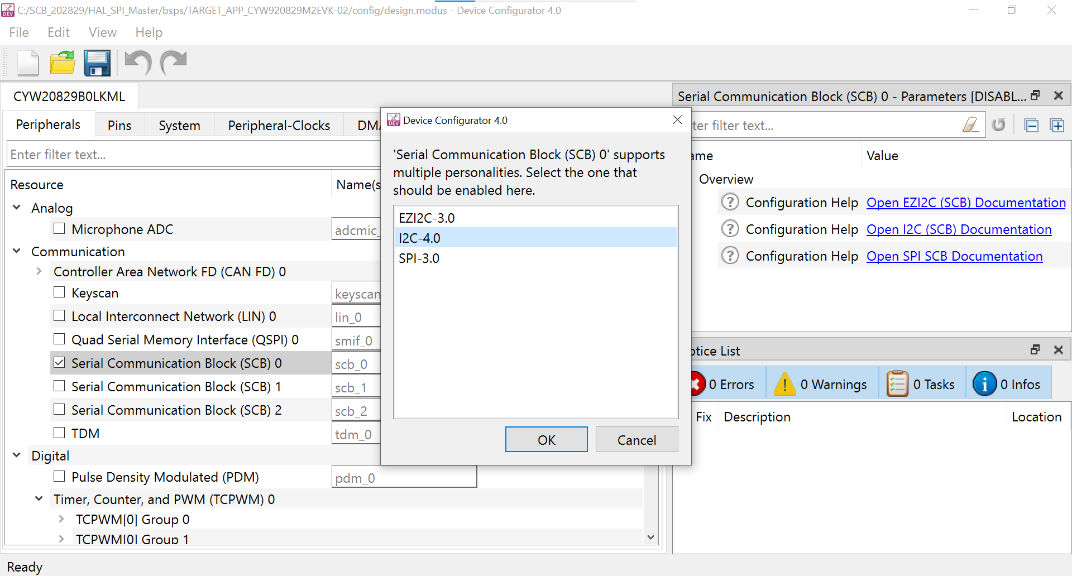
- Select the checkbox next to the SCB option
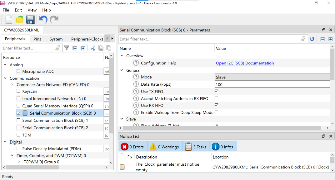
This action generates the initialization code. On the right side of the Device Configuration window, you can configure parameters such as Mode and Enable wakeup from Deep Sleep Mode(SCB0)
- Go to File and click Save before closing the Device Configurator. Additionally, the Device Configurator provides a Code Preview window that displays the defines and functions related to the SCB configuration
Applications and code example
SCB use cases are:
- SPI
- Communication with external peripheral
- Act as a peripheral device
- Wakeup from Deep Sleep
- UART
- Debug device with a PC
- Redirect Printf to use the UART
- I2C
- Communication with external peripheral
- Act as a peripheral device
- Wakeup from Deep Sleep
For example, see the following:
- HAL: SPI master demonstrates the use of a SPI (HAL) resource in master mode. The SPI master is configured to send command packets to control a user LED on the slave
- HAL: SPI slave demonstrates the use of a SPI (HAL) resource in slave mode. The SPI slave is configured to receive command packets to control a user LED on the kit
- Hardware Abstraction Layer (HAL): I2C master demonstrates the use of the I2C resource in HAL in master mode. The I2C master is configured to send command packets to control a user LED on the slave
- Hardware Abstraction Layer (HAL): I2C slave demonstrates the use of the I2C resource in HAL in slave mode. The I2C slave is configured to receive command packets to control a user LED on the kit
- HAL: Hello world demonstrates a simple UART communication by printing the "Hello world" message on a terminal and blinking an LED using a timer resource
TCPWM/Timer
The Timer, Counter, Pulse Width Modulator (TCPWM) block in CYW20829 uses a 16- or 32-bit counter, which can be configured as a timer, counter, pulse width modulator (PWM), or quadrature decoder.
The block can be used to:
- Measure the period and pulse width of an input signal (timer)
- Find the number of times a particular event occurs (counter)
- Generate PWM signals, or decode quadrature signals
This chapter explains the features, implementation, and operational modes of the TCPWM block. TCPWM supports operation in Active, Low power Active, Sleep and Low power Sleep power modes.
Features
- The TCPWM block supports the following operational modes:
- Timer-counter with compare
- Timer-counter with capture
- Quadrature decoding
- Pulse width modulation
- Pseudo-random PWM
- PWM with dead time
- Up, Down, and Up/Down counting modes
- Clock prescaling (division by 1, 2, 4, ... 64, and 128)
- 16- or 32-bit counter widths
- Double buffering of compare/capture and period values
- Underflow, overflow, and capture/compare output signals
- Complementary output for PWMs
- Supports interrupt on:
- Terminal count: Depends on the mode; typically occurs on overflow or underflow
- Capture/compare: The count is captured to the capture register or the counter value equals the value in the compare register
Description
To enable and disable the TCPWM block, use the TCPWM_CTRL_SET and TCPWM_CTRL_CLR register bits, respectively. Use these registers to avoid race-conditions on read-modify-write attempts to the TCPWM_CTRL register, which controls the enable/disable fields of the counters.
Block diagram
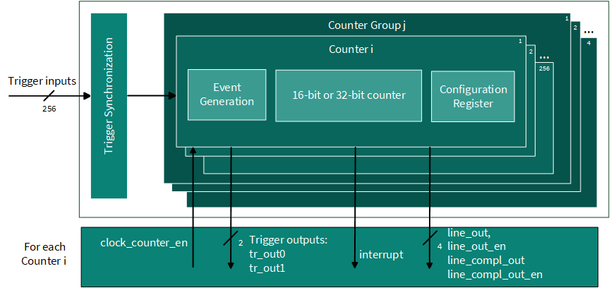
- The TCPWM block can contain up to 32 counters. Each counter can be 16- or 32-bit
wide. The three main registers that control the counters are:
- TCPWM_CNT_CC is used to capture the counter value in CAPTURE mode. In all other modes, this value is compared to the counter value
- TCPWM_CNT_COUNTER holds the current counter value
- TCPWM_CNT_PERIOD holds the upper value of the counter. When the counter counts for n cycles, this field should be set to n–1
The number of 16- and 32-bit counters are device-specific. For more details, see the device datasheet. In this chapter, a TCPWM refers to the entire block and all the counters inside. A counter refers to the individual counter inside the TCPWM. Within a TCPWM block, the width of each counter is the same. TCPWM has following interfaces:
- I/O signal interface: Consists of input triggers (such as reload, start, stop, count, and capture) and output signals (such as pwm, pwm_n, overflow (OV), underflow (UN), and capture/compare (CC)). All of these input signals are used to trigger an event within the counter, such as a reload trigger generating a reload event. The output signals are generated by internal events (underflow, overflow, and capture/compare) and can be connected to other peripherals to trigger events
- Interrupts: Provides interrupt request signals from each counter, based on TC or CC conditions
TCPWM counters
Each TCPWM counter can have its own clock source and the only source for the clock is from the configurable peripheral clock dividers generated by the clocking system. To select a clock divider for a particular counter inside a TCPWM, use the CLOCK_CTL register from the PERI register space.
Each TCPWM block has 14 Trigger_In signals, which come from other on-chip resources, such as other TCPWMs, SCBs, or DMA. The Trigger_In signals are shared with all counters inside of one TCPWM block. Use the Trigger Mux registers to configure which signals get routed to the Trigger_In for each TCPWM block. Two constant trigger inputs, ‘0’ and ‘1’, are available in addition to the 14 Trigger_In. For each counter, the trigger input source is selected using the TCPWM_CNT_TR_CTRL0 register. Each counter can select any of the 16 trigger signals to be the source for any of the following events:
- Reload
- Start
- Stop/Kill
- Count
- Capture/swap
Each counter can generate three trigger output events. These trigger output events can be routed through the trigger mux to other peripherals on the device.
The three trigger outputs are:
- Overflow (OV)
- Underflow (UN)
- Compare/Capture (CC)
The TCPWM block provides a dedicated interrupt output for each counter. This interrupt can be generated for a terminal count (TC) or CC event. A TC is the logical OR of the OV and UN events.
Each counter has two outputs: pwm (line_out) and pwm_n (line_compl_out) (complementary of pwm). Note that the OV, UN, and CC conditions are used to drive pwm and pwm_n by configuring the TCPWM_CNT_TR_CTRL2 register.
The TCPWM block works in Active and Sleep modes. The TCPWM block is powered from VCCD. The configuration registers and other logic are powered in Deep Sleep mode to keep the states of configuration registers.
TCPWM operating modes
TCPWM supports six function modes: Timer, Capture, quadrature Decoder, Pulse Width Modulation (PWM), PWM with dead time insertion (PWMDT) and Pseudo random PWM (PWM_PR). The TCPWM driver is structured to map these functional modes to four high-level operating modes:
- Timer/counter mode:
The timer mode is used to measure the time taken for an event or the time difference between two events. The timer functionality increments and decrements a counter between ‘0’ and the value stored in the PERIOD register. When the counter is running, the count value stored in the COUNTER register is compared with the compare/capture register (CC). When the counter changes from a state in which COUNTER equals CC, the cc_match event is generated
- Capture mode:
The capture functionality increments and decrements a counter between ‘0’ and PERIOD. When the capture event is activated, the count value in the COUNTER register is copied to CC (and CC is copied to CC_BUFF). The capture functionality is used to measure the pulse width (connected as one of the input triggers and used as a capture event)
- PWM:
- Pulse Width Modulation mode (PWM)
The PWM can output a left, right, center, or asymmetrically-aligned PWM. Incrementing or decrementing a counter between ‘0’ and PERIOD and comparing the counter value COUNTER with CC generates the PWM signal. When COUNTER equals CC, the cc_match event is generated. To generate a pulse-width modulated signal, use the cc_match event along with overflow and underflow events. Two pulse-width modulated signals, pwm and pwm_n, are outputs from the PWM
To generate the PWM output signals, use the underflow, overflow, and cc_match events. Each of these events can be individually set to INVERT, SET, or CLEAR pwm_dt_input. The PWM behavior depends on the PERIOD and CC registers. The software can update the PERIOD_BUFF and CC_BUFF registers without affecting the PWM behavior. This is the main rationale for double-buffering these registers
- PWM with Dead Time mode (PWMDT)
The PWMDT functionality is the same as the PWM functionality; however, the following are the differences:
- PWM_DT supports dead time insertion; PWM does not support dead time insertion
- PWM_DT does not support clock pre-scaling; PWM supports clock pre-scaling
- PWM Pseudo-Random mode (PWMPR)
The PWM_PR functionality changes the counter value using the linear feedback shift register (LFSR). This results in a pseudo random number sequence. A signal similar to PWM signal is created by comparing the counter value COUNTER with CC. The generated signal has different frequency or noise characteristics than a regular PWM signal
- Pulse Width Modulation mode (PWM)
- Quadrature decoder mode:
The Quadrature functionality increments and decrements a counter between ‘0’ and 0xFFFF or 0xFFFFFFFF (32-bit mode). Counter updates are under the following quadrature signal input control:
-
- The index input is used to indicate an absolute position
- The phiA and phiB inputs are used to determine a change in position (the rate of change in position can be used to derive speed)
Software usage
This section describes the TCPWM software usage using HAL and PDL API’s. Additionally, it explains the Device Configurator usage.
For more details, see the TCPWM PDL APIs in the following:
Device Configurator
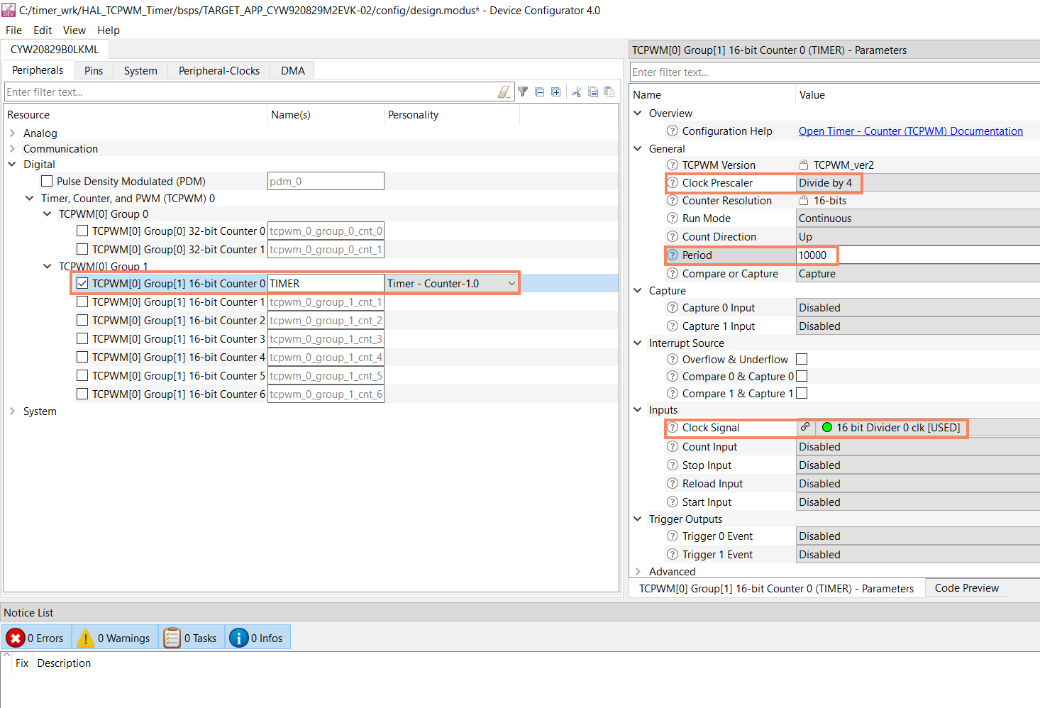
From the Device Configurator, select 32-bit counter or 16-bit counter (see Figure 29). TCPWM can be configured in any one of the operating mode.
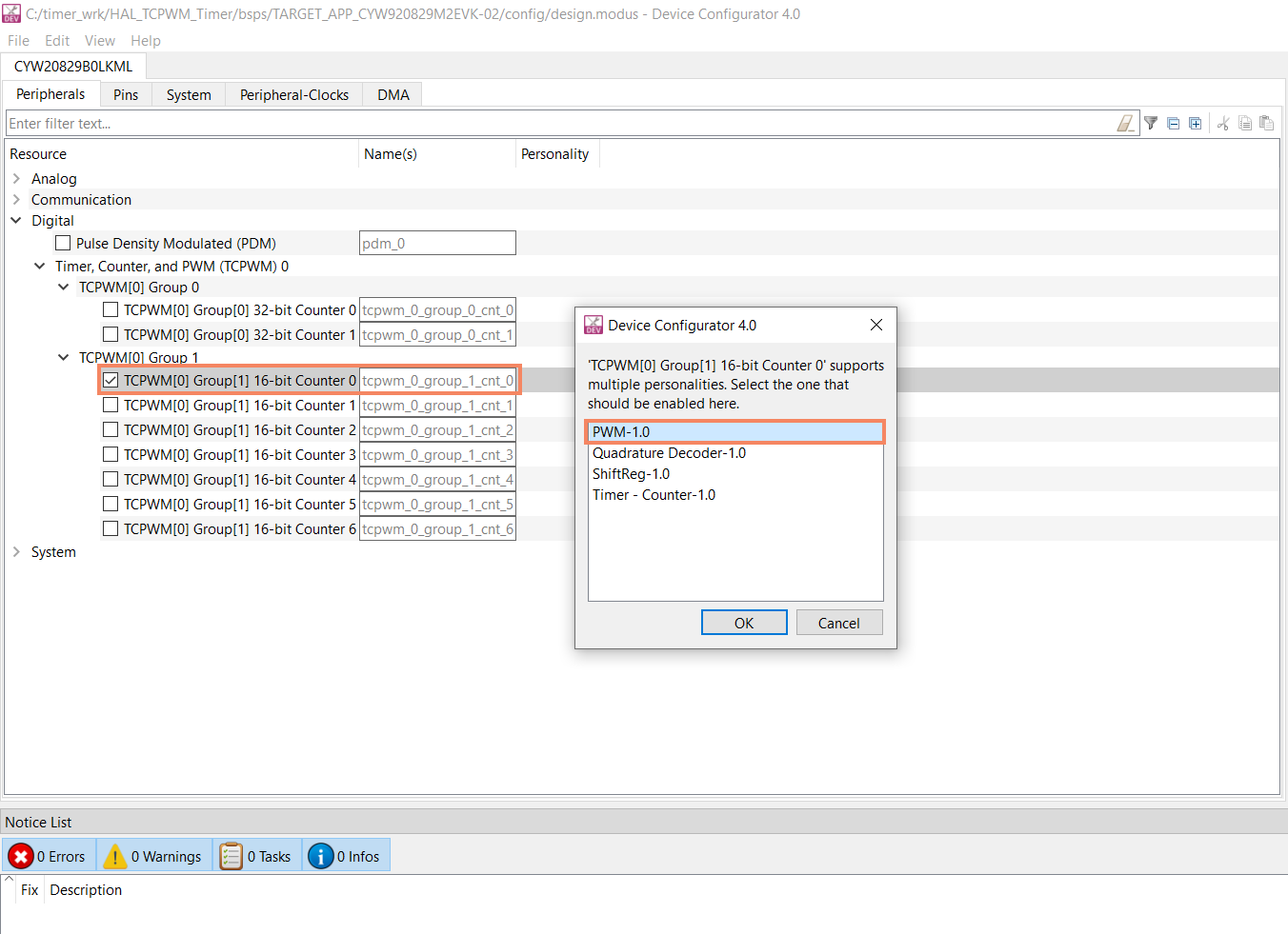
For example, configure the Timer/Counter mode using the following parameters (see Figure 30):
- TCPWM[0] Group [1] 16-bit Counter 0 = Timer and Timer – Counter- 1.0
- Clock Prescaler = Divide by 4
- Period = 10000
- Clock signal = 16 bit Divider 0 clk [USED]
Application and code examples
TCPWM can be used in multiple operations anything bound with timing requirements.
The following are the typical applications:
- Timer/Counter: Used in various applications like LED blinking and Events handling
- PWM: Used in many lighting and motor control applications
- Quadrature Decoder: Used in position sensing (e.g., Mouse scroll wheel)
For more details, see the following:
Watchdog timer (WDT)
The WDT driver provides a low-level interface to the WDT Hardware block. The purpose of using WDT is to recover from CPU or firmware failure by generating a device reset (WRES). It generates periodic interrupts and prevents the system from crashing by resetting the device. The WDT can be used as an interrupt source or a wakeup source in low-power modes.
Features
The WDT component provides the following features:
- CLK_LF as the input clock source
- Periodic Interrupt or wakeup generation in Active, Sleep, Deep Sleep, and Hibernate power modes
- Device reset generation if not serviced within a configurable interval
Description
WDT has the capability to issue counter match interrupts and trigger a device reset in the absence of interrupt handling. WDT main purposes can be categorized into two use cases:
- The first involves utilizing the WDT to recover from a CPU or firmware failure. By configuring a timeout period within the Watchdog timer, if the specified time elapses without receiving a signal, the device undergoes a reset (WRES)
- The second is used to generate periodic interrupts. Instead of performing a device reset, the WDT can generate an interrupt. This interrupt can be handled by the Interrupt Service Routine (ISR) either as a periodic interrupt or as an early indication of a firmware failure, allowing the watchdog to be cleared
In CPU Active power modes, the watchdog counter has the capability to issue interrupt requests to the CPU, while in CPU Sleep and Deep Sleep power modes, it can send interrupt requests to the wakeup interrupt controller (WIC).
- Active mode: In this mode, WDT is capable of sending an interrupt to the CPU, CPU acknowledges the interrupt request and proceeds to execute the Interrupt Service Routine (ISR). The ISR is responsible for clearing the interrupt
- Sleep or Deep Sleep mode: The interrupt request from the WDT is directly transmitted to the WIC. The WIC is responsible for awakening the CPU. Once the CPU acknowledges the interrupt request, it proceeds to execute the ISR. The ISR firmware is responsible for clearing the interrupt within its operations
- Hibernate mode: Few peripherals such as the WDT remains active. Any interrupt that aims to wake up the device while in this mode will lead to a device reset. There is no specific interrupt service routine or mechanism associated with this particular mode
Block diagram
This section provides an overview of the functionality of the WDT. The WDT consists of a wraparound up-counter that continuously counts. The counter is driven by the CLK_LF clock. The timer is capable of generating an interrupt when it matches a specified value and triggering a reset event after the occurrence of the third unhandled interrupt. The number of bits utilized for the match comparison can be configured.
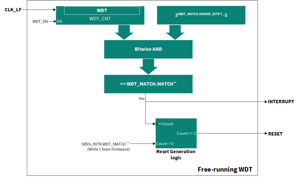
When WDT is enabled, it increments its counter with each rising edge of the CLK_LF signal. An interrupt is generated when the counter value matches the value stored in the MATCH bits of the WDT_MATCH register. Note that the match event does not reset the WDT counter; it continues counting until it reaches the 22-bit boundary (0x3FFFFF). At this point, it wraps around to ‘0’ and starts counting up again. The match interrupt is generated every time the counter value equals the match value, and the WDT_MATCH bit of the SRSS_INTR register is set to indicate this interrupt occurrence. To clear the interrupt and reset the watchdog, a ‘1’ must be written to the same bit (WDT_MATCH bit of SRSS_INTR). If the firmware fails to clear the interrupt for two consecutive occurrences, the third interrupt results in a device reset. Use the WDT_EN bit to enable or disable the WDT. The WDT provides an option to set the number of bits to be used for comparison. Use the IGNORE_BITS of the WDT_MATCH register to configure the number of LSBs to ignore from the 22-bit count value while performing the match.
Software usage
This section describes the software usage of WDT using HAL APIs and PDL APIs. For more details, see the WDT HAL APIs and PDL APIs in the following:
Sequence diagram
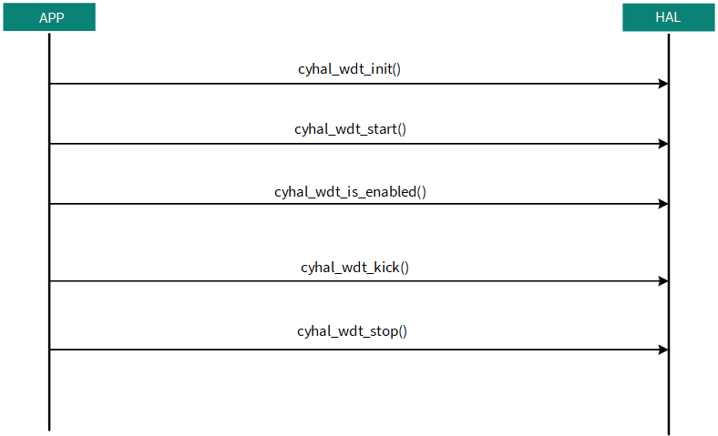
- Initialize the WDT using the following
function:
cyhal_wdt_init() - Start (enable) the WDT using the following
function:
cyhal_wdt_start() - Use the following command to check whether the WDT is
enabled:
cyhal_wdt_is-enabled() - Reset the device using the following
function:
cyhal_wdt_kick()This function must be called periodically to prevent the WDT from timing out and resetting the device
- Disable the WDT using the following
function:
cyhal_wdt_stop()
Device Configurator
WDT is not supported in Device Configurator.
Applications and code examples
WDT use cases are:
- Generate device reset
- Generate interrupts
- Generate periodic interrupts
For example, HAL: Watchdog Timer demonstrates how to set up a WDT using the WDT HAL resource. The WDT resets the device if it is not serviced or “kicked” within the configured timeout interval. This helps in recovering the program from an unintended lock up.
MCWDT
The MCWDT component offers an interface for configuring one MCWDT hardware block. Each block consists of three counters that can be customized for different system utility functions, including a free-running counter, periodic interrupts, or watchdog reset. Note that besides the MCWDTs, each device also has a standalone watchdog (WDT) that can be utilized to generate a watchdog reset or periodic interrupts.
Features
- Device reset generation if not serviced within a configurable interval
- Two 16-bit counters that can be free running, generate periodic interrupts, or generate a watchdog reset
- One 32-bit counter that can be free running or generate periodic interrupts
- Periodic interrupt/wake up generation in LP/ULP Active, LP/ULP Sleep, and Deep Sleep power modes
- All counters are clocked by CLK_LF
Description
The main purpose of MCWDT is to generate periodic CPU interrupts and function as a free-running timer. MCWDT has the capability to produce up to three periodic interrupts. Each MCWDT generates a single combined interrupt. An Interrupt Service Routine (ISR) can handle this interrupt either as a periodic interrupt or as an early indication of a firmware failure requiring the watchdog to be cleared. An alternative application of MCWDT is as a watchdog, serving to recover from CPU or firmware failures. The CLK_LF serves as the clock source for all the counters, enabling their operation in Active, Sleep, and Deep Sleep modes. However, note that Hibernate mode is not supported for these counters.
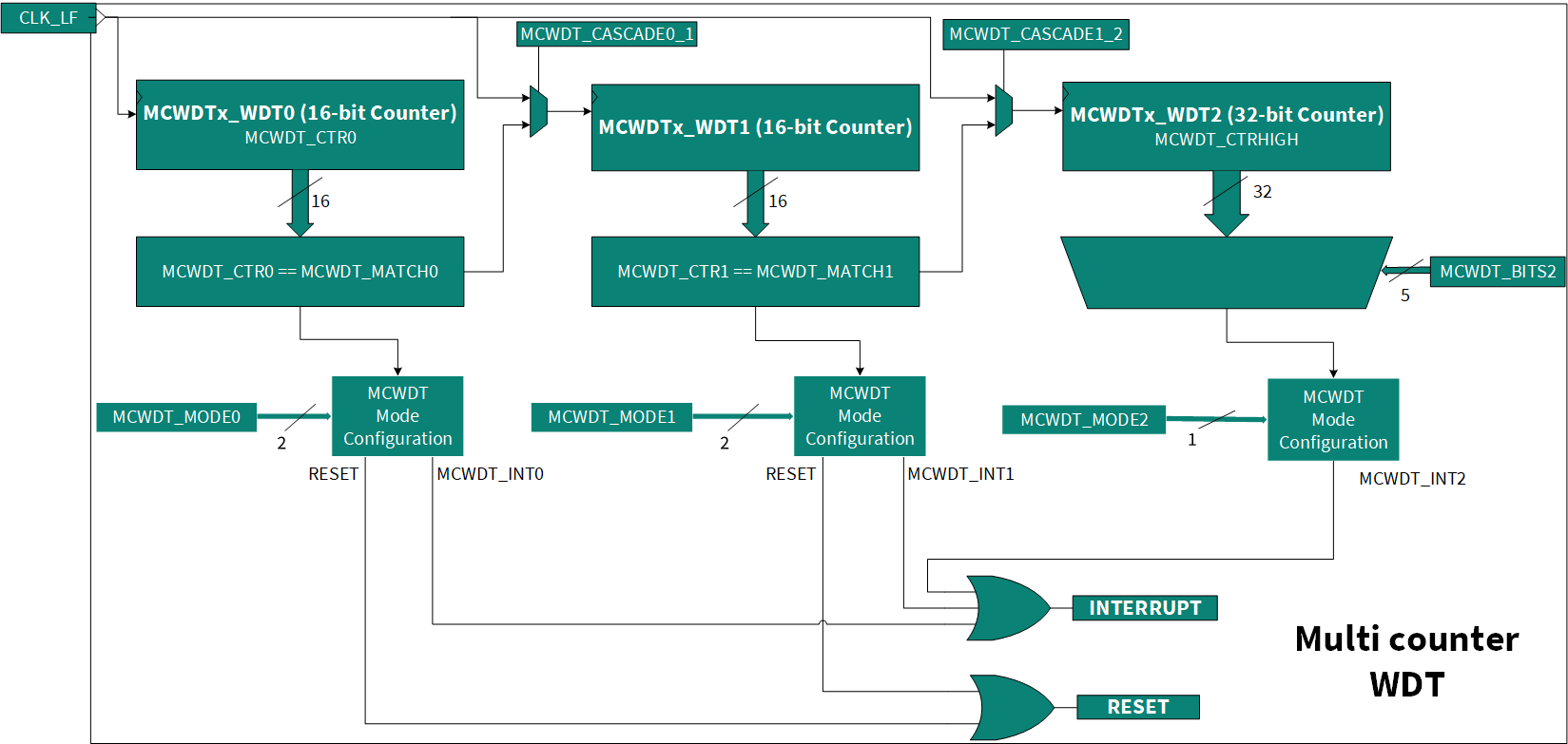
Block diagram
The functional overview of a multi-counter WDT block in the 20829 MCU reveals the inclusion of one MCWDT (Multi-Counter Watch Dog Timers) block. This MCWDT block consists of two 16-bit counters, namely MCWDTx_WDT0 and MCWDTx_WDT1, along with one 32-bit counter known as MCWDTx_WDT2. These counters can be configured to operate independently or in a cascade configuration, allowing for a maximum counter size of 64 bits. MCWDTx_WDT0 and MCWDTx_WDT1 are 16-bit up counters, which can be configured to be a 16-bit free-running counter or a counter with any 16-bit period. These counters can be used to generate an interrupt or reset the device. The MCWDTx_WDT2 is a 32-bit free-running counter, which can be configured to generate an interrupt. All the counters are synchronized by CLK_LF.
Software usage
This section describes about the software usage of MCWDT using PDL APIs and device configurator. For more documentation refer the MCWDT PDL APIs provided in the below links.
Sequence diagram
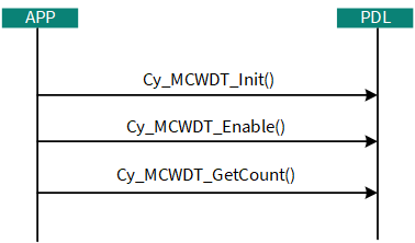
Using the MCWDT Peripheral Driver Library (PDL) resource, a MCWDT can report the current value of the specified counter when operating in free-running mode.
Device Configurator
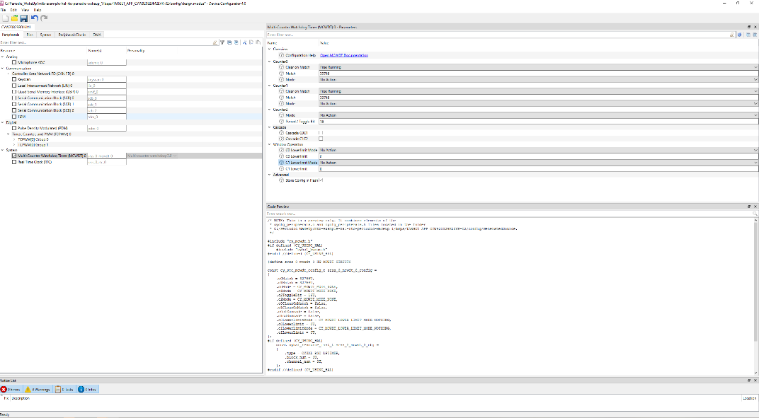
Do the following to initialize the MCWDT:
- Use the following methods to access the Device Configurator:
- Right-click on the project and select ModusToolbox™, and
then select Device Configurator
Or
- Click Device Configurator in the bottom left corner of the Quick Panel of ModusToolbox™
- Right-click on the project and select ModusToolbox™, and
then select Device Configurator
- Navigate to the Peripheral tab in the Device Configurator
- Select the checkbox next to the MCWDT option.
This action generates the initialization code. On the right side of the Device Configuration window, you can configure Counter0, Counter1, and Counter2
- Go to File and click Save before closing the Device Configurator. Additionally, the Device Configurator provides a Code Preview window that displays the defines and functions related to the MCWDT configuration
Applications and Code example
MCWDT use cases are:
- Periodic Interrupt Generation
- Reset Generation
- Interrupt Generation
- Free running timer
For example, HAL: Low-power timer demonstrates how to configure a low-power timer to measure the timing between events in free-running mode using the LPTimer HAL resource.
Real time clock (RTC)
RTC is a hardware component that is used to keep track of the current time and date as well as the ability to trigger a callback at a specific time. RTCs are commonly used in electronic devices such as computers, smartphones, digital cameras, microwave ovens, washing machines, clocks and other home appliances, IoT, and activity trackers where an accurate and reliable time reference is required. The RTC operates independently of the main system clock and continues to keep track of time even when the system is turned OFF or in Sleep mode. The RTC typically has a battery backup to maintain the timekeeping function; therefore, it can retain the time and date information even when the main power source is disconnected. RTC circuits usually include a crystal oscillator, a counter, and a register for storing the time and date information.
Features
The RTC component supports the following features:
- BCD time and date format
- Configurable alarm
- Century interrupt feature
- Configurable DST
- 12-Hour/24-Hour time format
- Automatic leap year compensation
- Option to drive the RTC by an external 50-Hz or 60-Hz clock source while internal watch crystal oscillator is the default source
Description
The RTC is comprised of eight fields, namely RTC_SEC, RTC_MIN, RTC_HOUR, CTRL_12HR, RTC_DAY, RTC_DATE, RTC_MON, and RTC_YEAR, all of which are encoded in binary-coded decimal (BCD) format. BCD encoding uses four bits to represent a single decimal digit. The RTC supports both 12-hour and 24-hour time formats, with the "hours" field capable of displaying AM/PM flags. The RTC hardware automatically compensates for leap years, eliminating the need for manual adjustment. Leap years are defined as years that are divisible by 4 or 400 but not by 100.
- To Read and Write, set the READ bit and WRITE bit in the BACKUP_RTC_RW register
- The RTC's Alarm feature enables the generation of an interrupt that can wake up the system from Sleep, Deep Sleep, and Hibernate power modes. It consists of six fields that correspond to the RTC fields: Month/Date, Day-of-Week, and Hour:Minute:Second. This allows the RTC to generate an interrupt when the RTC time matches the time set in the ALARM registers. The RTC component physically provides two alarm functions that can trigger an SRSS backup interrupt to prompt an appropriate action on time
- The RTC component offers two modes for DST: fixed date and relative date. When DST is enabled, the alarm2 block is reserved for executing DST start or stop actions. DST can be optionally enabled and supports any start and end date, which can either be a fixed date such as March 24th or a relative date
Block diagram
The RTC comprises two distinct blocks. The AHB RTC user registers contain all RTC settings and synchronize with the actual RTC register. However, the AHB RTC user registers do not update automatically. Instead, they are copied on-demand when a read transaction is initiated from the actual RTC register. To avoid stalling the actual RTC, you are only allowed to access the AHB RTC user register.
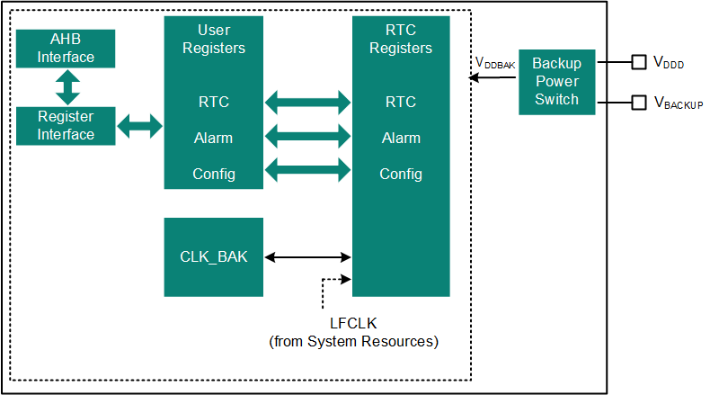
The components of the RTC are:
- Crystal oscillator: Generates a clock signal that is used by the counter to keep track of the time and date
- Counter: Increments the values of the time and date registers accordingly
- Registers: Store the time and date information
- Battery backup: Maintain the timekeeping function even when the power source is disconnected
- Control logic: Manages the operation of the RTC circuit and interfaces with the rest of the system
- Interface: Provides a way to set the time and date, read the time and date, and configure other RTC functions
Software usage
This section describes the software usage of RTC using PDL and HAL APIs and Device Configurator. For more details on RTC HAL APIs and PDL APIs, see the following:
Sequence diagram
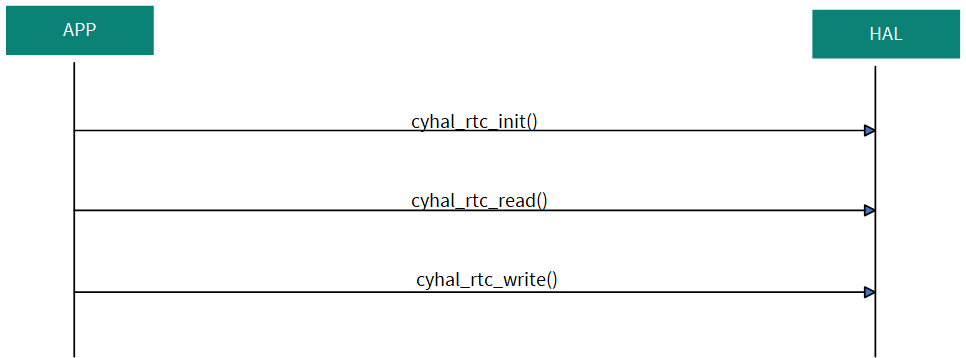
Use case 1: Receive and set the time in the RTC using the RTC HAL API.
- Initialize the RTC peripheral using the following
function:
cyhal_rtc_init()This initialization step does not alter the RTC's state but grants access to it
- Write the specified time and date to the RTC peripheral using the following
function:
cyhal_rtc_write()Conversely, the following function gets the current time and date from the RTC peripheral:
cyhal_rtc_read()
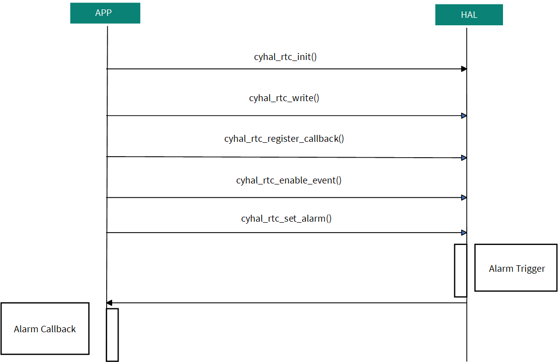
Use case 2: Set the alarm in the RTC using RTC HAL API.
- Initialize the RTC peripheral using the following
function:
cyhal_rtc_init()This initialization step does not alter the RTC's state but grants access to it
- Write the specified time and date to the RTC peripheral using the following
function:
cyhal_rtc_write()Conversely, the following function gets the current time and date from the RTC peripheral:
cyhal_rtc_read() - Register an RTC event callback handler using the following
function:
cyhal_rtc_register_callback()This enables a specific function to execute when an RTC event occurs
- Configure RTC events using the following
function:
cyhal_rtc_register_callback()This allows you to define the desired behavior for different RTC events
- Set an alarm (interrupt) for the specified time and date using the RTC peripheral
using the following function:
cyhal_rtc_set_alarm()This allows you to schedule an alarm that will trigger an interrupt when the specified time and date are reached
Device Configurator
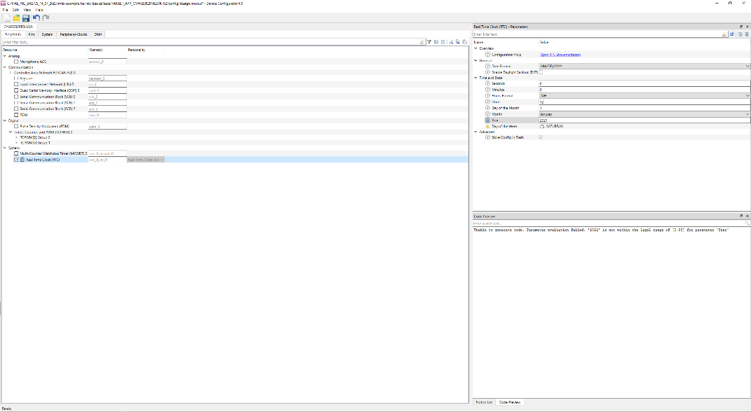
Do the following to initialize the RTC:
- Use the following methods to access the Device Configurator:
- Right-click on the project and select ModusToolbox™, and
then select Device Configurator
Or
- Click Device Configurator in the bottom left corner of the Quick Panel of ModusToolbox™
- Right-click on the project and select ModusToolbox™, and
then select Device Configurator
- Navigate to the Peripheral tab in the Device Configurator
- Select the checkbox next to the RTC option
This action generates the initialization code. On the right side of the Device Configuration window, you can configure Date Format, Enable DST, Time, and Date for the RTC
- Go to File and click Save before closing the Device
Configurator
Additionally, the Device Configurator provides a Code Preview window that displays the defines and functions related to the RTC configuration
Applications and code examples
RTC use cases are:
- RTC time keeping and time-stamping
- Set daily alarm or one time alarm
- RTC as a stopwatch
- DST adjustment
- Generate one sec interrupts
For example, see the following:
- HAL: RTC periodic wakeup demonstrates how to enter the Deep Sleep and Hibernate modes and wakeup using the RTC alarm
- HAL: Real-time clock basics demonstrates the usage of the real-time clock (RTC) in the Infineon MCU. It shows how to get and set the time in the RTC using the RTC HAL API. The example also supports the daylight saving time (DST) feature. A UART interface is used to input the time and configure the RTC
Datawire
A Direct Memory Access (DMA) block is specifically designed for data movement and is more power efficient than the CPU for transferring large data blocks. The DMA block provides an independent data transfer engine, which offloads the CPU usage on data transfer use cases. The DMA block in CYW20829 implements a data transfer engine with different configuration options that lets the DMA block be used in different data transfer use cases. This chapter describes the different DMA configurations and use cases. The DMA engine in CYW20829 called Datawire (DW) is specifically designed for transferring small data blocks, typically between peripherals and memory, to offload the CPU from any data transfer with peripherals.
Features
The DMA (Datawire) hardware block has the following features:
- Transfers the data between peripherals to memory without involving the CPU core
- One Datawire block (DW0) that supports up to 16 channels
- Supports multiple instances of DMA channel
- Four levels of priority for each channel
- Various attributes of DMA are configurable through software called DMA descriptors
- DMA Descriptors are defined in memory and referenced to the respective DMA channels
- Supports single-shot, one-dimensional (1-D), and two-dimensional (2-D) transfer modes using DMA descriptor
- Supports transfers up to 65536 data elements per descriptor
- Configurable source and destination address increments
- Supports 8-bit, 16-bit, and 32-bit data widths at both source and destination
- Descriptors can be chained to other descriptors in memory
- Configurable input/output trigger and interrupt generation for each descriptor
- Available in Active and Sleep power mode
Description
DMA transfers the data to and from the memory, peripherals, and registers. These transfers occur independently from the CPU. DMA can be configured to perform multiple independent data transfers. A channel manages all data transfers. There can be up to 32 channels in the DMA. Datawire focuses on peripheral-to-memory and memory-to-peripheral data transfers (however, it can also perform memory-to-memory data transfers). It is designed to achieve low latency for a large number of channels. It uses a single-data transfer engine that is shared by all channels.
Block diagram
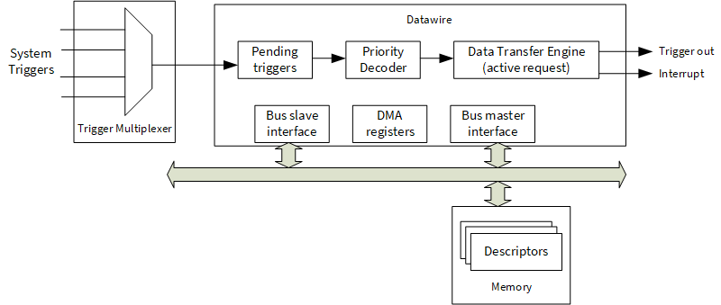
Implementation
- DMA Channels
A single DMA hardware block can support many DMA channels that may be triggered by independent and unrelated events. CYW20829 has one DMA block that supports up to 16 channels. Each DMA channel has a trigger input, trigger output, and interrupt output line. Interrupt signals are routed to individual interrupt lines in the respective CPU. Trigger signals to and from DMA channels are routed through a trigger multiplexer block, which has a device-specific architecture. The trigger multiplexer block enables routing of trigger signals from different peripherals to the DMA block and routing trigger outputs back to other peripherals
The DMA channels has one of the following four channel states at any given time:
- Disabled: Channel is disabled
- Blocked: Channel is enabled and is waiting for a trigger to initiate the data transfer
- Pending: The channel is enabled and has received an active trigger. In this state, the channel is ready to initiate a data transfer but waiting for it to be scheduled
- Active: The channel is enabled, has received an active trigger and has been scheduled. It is actively performing data transfer(s). If there are multiple channels pending, the highest priority pending channel gets scheduled
- Channel priorities and preemption
The DMA channels can be assigned priorities, and preemption can be enabled to handle higher-priority transfers. A channel is assigned a priority between ‘0’ (0’ being the highest priority) and ‘3’ (‘3’ being the lowest priority). Channels with the same priority constitute a priority group. Priority decoding determines the highest-priority pending channel. This channel is determined as follows
- The highest-priority group with pending channels is identified
- Within this priority group, round-robin arbitration is applied. Round-robin arbitration (within the priority group) provides the highest priority to the lower channel indices (within the priority group)
However, if there is a low-priority channel already active and is in the middle of a large transfer, a pending higher-priority channel cannot become active. This can hold the execution of a higher-priority channel. This can be a problem when the higher-priority channel caters to a data transfer that is time-sensitive. Figure 41 shows this condition in the case of channel without preemption. To address this, there is an additional configuration parameter in the DMA channel called “preemptable”. This parameter allows a higher-priority channel to preempt the currently active low-priority channel. If a channel has preemptable enabled, any other channel with a higher priority can preempt the channel. This means that when the DMA channel is in the middle of a transfer, a higher-priority channel request will stop the current transfer after completing the current atomic transfer, keep the channel pending, and then start the higher-priority channel. The data width parameter determines the size of an atomic transfer. Only when the high-priority channel is completed, the low-priority channel may resume. A low-priority preemptable channel can get preempted multiple times during a single transfer.
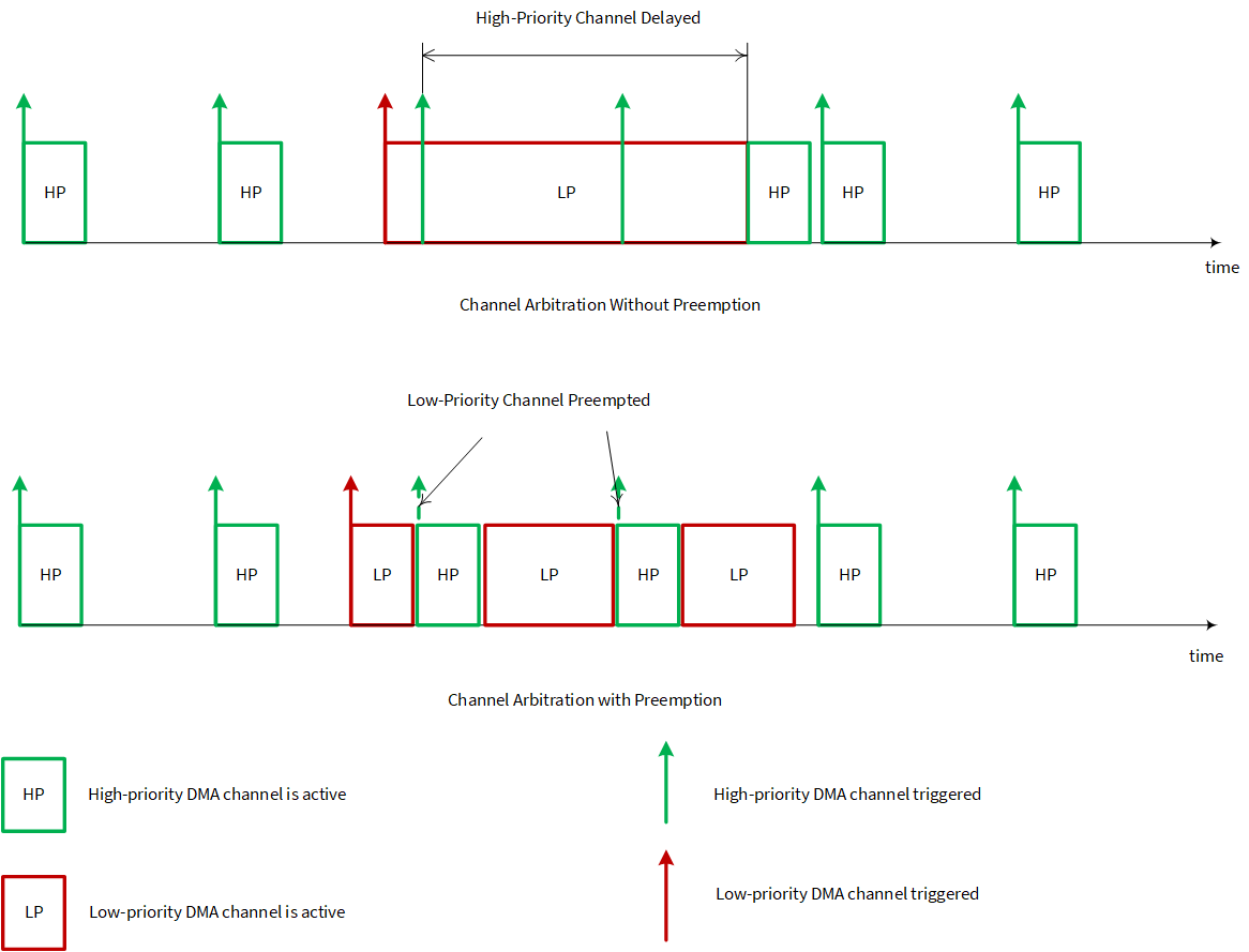
Preemption is useful only in cases when there are low-priority channels with no constraints of transfer times and there are high-priority channels that are time-sensitive and cannot be held hostage by other on-going transactions. Note that preemption can cause significant delay in low-priority transfers, if:
- There are multiple frequent requests from high priority channels
- The time taken for a high-priority transfer is too long
There are multiple bus masters in the CYW20829 device. A DMA channel may have the highest priority in its DMA hardware block, but that does not guarantee its performance on the bus when arbitrating with other bus masters. Sometimes, even a DMA channel’s descriptor fetch process can be delayed due to bus arbitration by other masters.
- Data transfer widths
The data width determines the width of the data being accessed at the source or destination. The DMA supports different data transfer widths, such as bytes, 2-byte words, and 4-byte words. This configuration is also responsible for the value of each increment of the X or Y loops which will be discussed below. Data widths must always be equal to the width supported by the device. For example, because all peripherals support 32-bit data width, if the source or destination of a transfer is a peripheral, the source or destination data width must be set to 32 bits.
Memory supports 8-bit, 16-bit, and 32-bit access. You can use larger data widths to increase throughputs or use smaller data widths to quantize the data size. For example, 8-bit data is being transferred from a communication block to the memory, the source data width must be 32 bits (because the source is a peripheral), but the destination can be 8 bits (because the destination is a memory location), which automatically truncates the higher 24 bits. This will enable a smaller memory footprint
- Descriptors
A descriptor describes the data transfer associated with a DMA channel and is stored in RAM or external flash with read-only attribute for CYW20829. The cy_stc_dma_descriptor_config_t structure in PDL driver cy_dma.h helps to configure the DMA descriptor. The descriptor defines different configurations of the transfer, such as size, data width, burst sizes, address increment schemes, and source and destination addresses. The descriptor is a structure of a specific type placed in a memory location. The pointer to this descriptor is associated with a DMA channel as part of its DMA channel configuration. When a DMA channel is active, the fetch its descriptor from the memory. Multiple descriptors can be associated with a DMA channel in a chained configuration
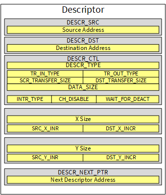
- Descriptor types (transfer modes - triggering schemes)There are three transfer modes for a DMA channel based on the transfer size (data element) that should be defined in the associated descriptor. A data element could be 1-byte, 2-byte or 4-byte word based on the width definition in the descriptor
- Single-shot (atomic) transfer: In this mode, the DMA channel can transfer only a single data element (byte, half word, and word). A trigger signal need to initiate each single transfer to the DMA channel
- 1D Transfer (X loop): In this mode, the DMA channel can transfer a single data element or the entire 1D transfer at a time. This mode is useful for buffer-to-buffer transfer or a peripheral-to-memory buffer transfer; it allows for multiple data elements to be transferred as defined in a descriptor. The descriptor can decide on the exact form of source and destination address increments
- 2D Transfer (Y loop): In this mode, the DMA channel can transfer a single data element, the entire 1D transfer at a time, or the entire 2D transfer at a time. mode allows for multiple 1D transfers to be defined in a single descriptor. This allows for a larger data count and allows for transfers of more complex data entities like array of data structures
- Types of transfers:
- 1-to-1 transfer: Enables the direct transfer of one data element from a source to a destination, triggered by interrupts
- 1-to-N transfer: Allows for the transfer of one data element to multiple destinations
- N-to-1 transfer: Enables the transfer of multiple data elements from multiple sources to a single destination
- N-to-N transfer: Enables the transfer of multiple data elements between multiple sources and destinations
- N-to-NxM transfer: Allows more complex transfers involving multiple sources and destinations
- Chaining descriptors (advanced use cases)
DMA blocks support descriptor chaining, which is useful if different types of transfers are to be done in a sequence. Each descriptor has the pointer to the next descriptor it must chain to, similar to a linked list. There is no limit on the number of descriptors you can chain. One of the greatest advantages of chaining is that each descriptor can have a different configuration including different source and destination addresses, trigger settings, interrupt settings, transfer modes, loops settings, and data widths. This allows the same DMA channel to implement multiple transfers of varying characteristics
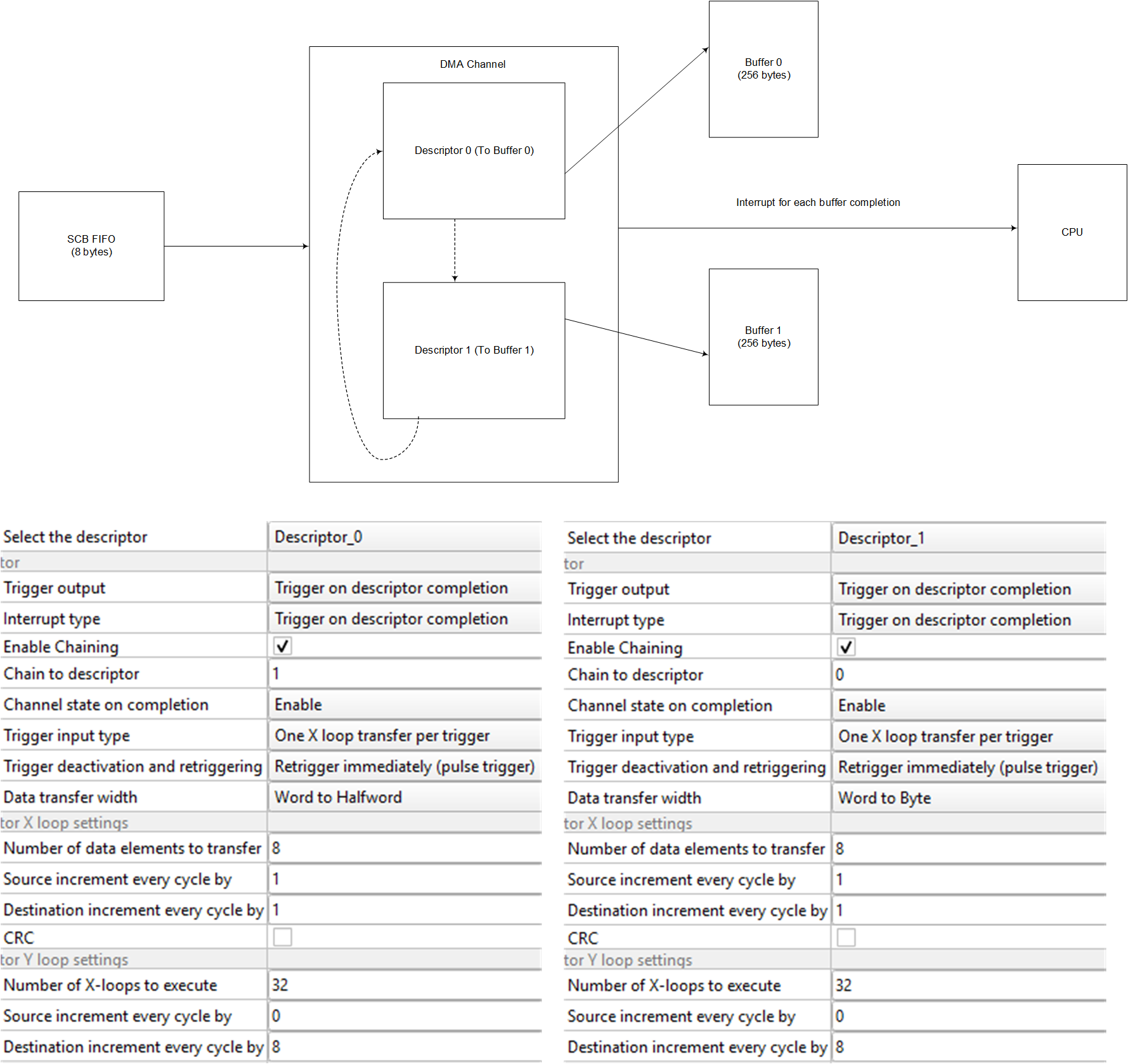
Figure 43 shows the double buffering, which is a good use-case for descriptor chaining. The input data is in the form of 8-byte blocks in the SCB FIFO, which needs to be moved to Buffer 0 or 1 for double buffering. The buffers are 256 bytes each and therefore can accommodate 32 FIFOs worth of data before overflowing. A single DMA channel is used for the transfer with two descriptors. Both descriptors are set up for a 2D transfer with the FIFO as the source. The X loop will cycle through the FIFO and therefore needs both source and destination increments. The Y loop handles the moving of 32 FIFOs. Descriptor 0 is set to chain to Descriptor 1 and vice versa. Descriptor 0 is configured to transfer to Buffer 0 and Descriptor 1 to Buffer 1. Once Descriptor 0 is completed, the control automatically transfers to Descriptor 1 due to chaining. This will ensure the continued transfer and double buffering. Each descriptor is also configured to interrupt the CPU at its transfer completion. This will inform the CPU that one buffer is available for processing
- Chaining DMA channels (advanced use cases)
In addition to chaining of descriptors in a single DMA channel, there are cases where it is useful to chain two DMA channels. To do this, one DMA channel’s trigger output is routed to the next DMA channel’s trigger input. Depending on the specific trigger multiplexer routing in CYW20829, only certain DMA channels will have the ability to chain. For more details on chaining restrictions of DMA channels, see the “Trigger Multiplexer” section
Trigger Multiplexer (TrigMUX)
It is important to understand Trigger Multiplexer for the typical usage of datawire. This subsection will provide the basic purpose of Trigger Multiplexer and will be detailed in a separate chapter dedicated for Trigger Multiplexer. Trigger Multiplexer is a series of multiplexers used to route the trigger signals from potential sources to destinations. CYW20829 has several SoC peripheral blocks; each of these blocks can be connected to other blocks through trigger signals. The trigger signals are digital signals generated by peripheral blocks to indicate an action such as completion of an event, state of FIFO level, etc. These trigger signals typically serve as initiator of other actions in other peripheral blocks. The trigger multiplexer can connect to any trigger signal emanating out of any peripheral block in CYW20829 and route it to any other peripheral to initiate an operation or change an ongoing operation at the destination peripheral block.
Software usage
For more details, see the RTC HAL APIs and PDL APIs provided in the following:
- DMA HAL : Hardware Abstraction Layer (HAL)
- DMA PDL : MTB CAT1 Peripheral Driver Library
Sequence diagram
Do the following to operate the DMA:
- Use the ModusToolbox™ Device Configurator to configure the
triggers, channels, and descriptors. This automatically generates the code in the cycfg_DMAs.h and cycfg_DMAs.c files.
Each descriptor will generate a descriptor structure called
CYBSP_DMA_PDM_Descriptor_2_config in the codeNote: This descriptor is not automatically initialized or allocated to the DMA channel. This must be done in user code as described in the following steps.
- A configuration structure “CYBSP_DMA_PDM_Descriptor_2_config” is generated, which has all descriptor configuration set in the Device Configurator. This can be used to initialize the descriptor CYBSP_DMA_PDM_Descriptor_2_config
- All channel-level configuration such as priority is configured in CYBSP_DMA_PDM_channelConfig. This structure can be used to initialize the channel
- Initialize the descriptor with the following function:
-
Cy_DMA_Descriptor_Init()
This step transfers all configuration to the descriptor
-
- Configure the source and destination addresses using the following
functions:
-
Cy_DMA_Descriptor_SetSrcAddress() -
Cy_DMA_Descriptor_SetSrcAddress()
-
- Initialize the channel and associate the descriptor to the channel with the
following function:
-
Cy_DMA_Channel_Init()
-
- Enable the channel using the following function:
-
Cy_DMA_Channel_Enable()
-
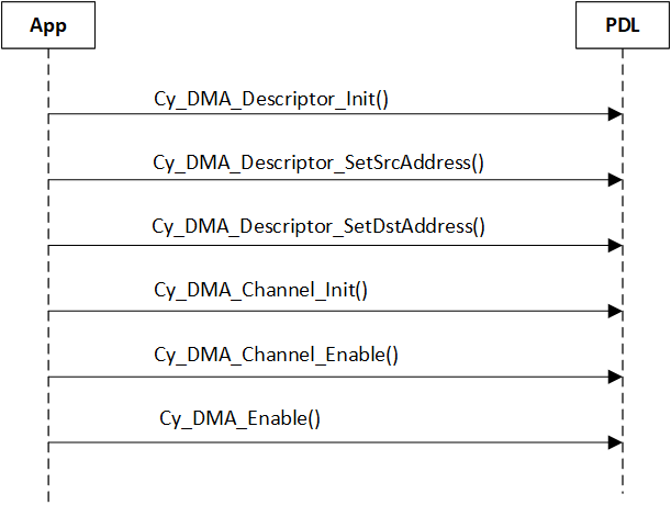
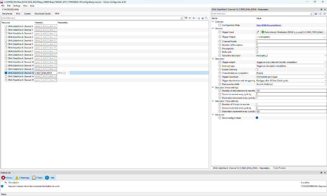
Device Configurator
Do the following to initialize the RTC:
- Access the Device Configurator via the following methods:
- Right-click on the project and select ModusToolbox™, and
then select Device Configurator
Or
- Click Device Configurator in the bottom left corner of the Quick Panel of ModusToolbox™
- Right-click on the project and select ModusToolbox™, and
then select Device Configurator
- Navigate to the DMA tab in the Device Configurator
Select the checkbox next to the required DMA Datawire channel option.
On the right side of the Device Configuration window, you can configure one or more DMA descriptors, DMA channel parameters, and the trigger input and output routing
Applications and code examples
DMA use cases are:
- Memory-to-peripheral data transfer without the CPU involvement
- Peripheral-to-memory data transfer without the CPU involvement
- Continuous data transfer operation from multiple peripherals-to-memory or peripherals while CPU is in Sleep mode
AIROC™ CYW20829 Voice Remote Reference Solution: This solution demo demonstrates the implementation of AIROC™ CYW20829 Voice Remote Reference Solution using the Infineon AIROC™ CYW20829 Bluetooth® LE MCU and ModusToolbox™ Software Environment. This application is designed to work on two platforms i.e., CYW920829-VR and CYW920829M2EVK-02.
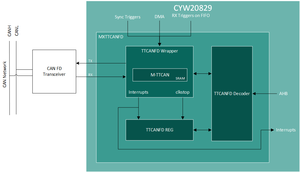
CAN
mxttcanfd(CAN FD Controller)is used as a CAN IP that supports CANFD and TTCAN. This IP implements CAN functionality with the integration of a third-party IP from BOSCH.
CAN is a broadcast type of bus and is a multi-master setup. All the nodes on the bus can hear all the transmissions. There is no way to send a message to just a specific node; all the nodes will invariably pick up the traffic. The CAN hardware, however, provides local filtering so that each node may react only on the interesting messages. CAN partially defines the services for the Physical and Data Link Layer of the OSI model.
Features
Major features of CAN FD are:
- Two configurable receive FIFOs (up to 64 buffers each)
- Configurable transmit FIFO
- Up to 64 dedicated receive buffers
- Up to 32 dedicated transmit buffers
- Shared message RAM
Description
The M_TTCAN operation is available in Active and Sleep power modes, and the IP is fully retained except for the Time Stamp counter in Deep Sleep power mode.
The following are the major blocks in CAN FD:
Dual clock sources
The M_TTCAN channel has two clock inputs:
- clk_can: Derived from the system peripheral clock dividers, it is used for the CAN (or CAN FD) operation
- clk_sys: Used for everything except CAN operations; for example, register accesses, SRAM accesses, and so on
Interrupt lines
The M_TTCAN channel provides two interrupt lines: interrupt0 and interrupt1. Interrupts from any source within the M_TTCAN channel can be routed either to interrupt0 or interrupt1. By default, all interrupts are routed to interrupt0.
MRAM – Message RAM
Each M_TTCAN group consists of one message RAM, and this message RAM is shared among the M_TTCAN channels belonging to that group. The M_TTCAN IP requires access to a MRAM to store in- and out-going messages and acceptance filters. The host CPU must also be able to access this MRAM. You must take care of distributing the MRAM to the channels of that group and prevent any overlapping distribution. The IP does not check internally if any MRAM region is overlapping for multiple channels of the group. The MRAM is ECC-protected with single-bit error correction and double-bit error detection feature. ECC errors and out-of-range accesses to the MRAM are reported to fault structures.
Message RAM contains Rx and Tx messages and the filter configurations. All messages go through MRAM to transmit or receive them.
M_TTCAN
All message handling functions are implemented by the Rx and Tx Handlers.
- Tx Handler: Transfers transmit messages from the message RAM to the CAN core and provides transmit status information
- Rx Handler: Manages message acceptance filtering, transfers received messages from the CAN core to a message RAM, and receives message status information
Timestamp generation
The M_TTCAN channel uses a 16-bit counter to record when messages are sent or received. This allows the application software to know the order in which events occurred.
Operation modes
The M_TTCAN's default operating mode after hardware reset is event-driven CAN communication without time triggers.
- CAN FD operation: The two variants of CAN FD frame transmission are:
- CAN FD frame without bitrate switching
- CAN FD frame where the control, data, and CRC fields are transmitted with a
higher bit rate than the beginning and end of the frame
The previously reserved bit in CAN frames with 11-bit identifiers and 29-bit identifiers will now be decoded as an FDF bit
- FDF = recessive signifies a CAN FD frame
- FDF = dominant signifies a classic CAN frame
In a CAN FD frame, the two bits following FDF, reserved bits (res), and bit rate switch (BRS) decide whether the bit rate inside the CAN FD frame is switched. A CAN FD bit rate switch signified by res is dominant, and BRS is recessive
- Restricted Operation mode:
In Restricted Operation mode, the node is able to receive data and remote frames and acknowledge valid frames, but it does not send data frames, remote frames, active error frames, or overload frames. In case of an error or overload condition, it does not send dominant bits; instead, it waits for the occurrence of a bus idle condition to resynchronize itself to the CAN communication.
The Restricted Operation mode can be used in applications that adapt themselves to different CAN bit rates. In this case, the application tests different bit rates and leaves the mode after it has received a valid frame.
- Bus Monitoring Mode:
In Bus Monitoring mode, the M_TTCAN is able to receive valid data frames and valid remote frames but cannot start a transmission. In this mode, it sends only recessive bits on the CAN bus. If the M_TTCAN is required to send a dominant bit (ACK bit, overload flag, or active error flag), the bit is rerouted internally so that the M_TTCAN monitors this dominant bit, although the CAN bus may remain in recessive state. The Bus Monitoring mode can be used to analyze the traffic on a CAN bus without affecting it through the transmission of dominant bits
Software usage
This section describes the software usage of CAN FD using PDL and device configurator. For more details on CANFD PDL APIs, see the following:
Prior to the main flow of transmission and reception of desired messages, you must initialize certain variables to define base values. Even though these values can be preconfigured in PDL flow, you can change them in code.
Members of structures such as “cy_stc_canfd_config_t CANFD_config” and “cy_stc_canfd_context_t canfd_context” must be initialized with desired values. For more details, see the “CAN FD on 20829” code example.
Sequence diagram
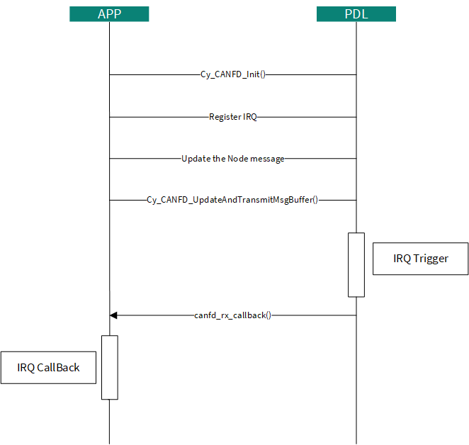
PDL interface
The Peripheral Driver provides an API to access the low-level registers of the CAN FD IP. The CAN FD PDL interface allows an easy configuration of the commonly used settings, the following are its functions:
- Initializes the required port: Enables available pin configurations specific to CAN FD
- Initializes the clock system and CANFD related prescaler: It is necessary to configure the frequency block used for the same
- Initializes the CANFD configuration block, like mode, bit rate, and so on
- Initializes the CANFD message filters: Required to set message ID filters
- Initializes the CANFD interrupt system
- Supports data transmission (object configuration and sending)
- Supports data reception (read-out of objects)
The CAN FD Peripheral Driver has an API to initialize the predefined structure type. You will need to pass this descriptor pointer as an instance into the channel initialization API. All the Peripheral Driver functions will have one parameter associated with them: the CAN FD hardware block number.
Device Configurator
For example. Figure 48, Figure 49, and Figure 50 show the values that can be filled in the Device Configurator to get the desired output.
The following figures show predefined values and you can change them if required.
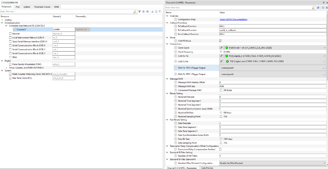
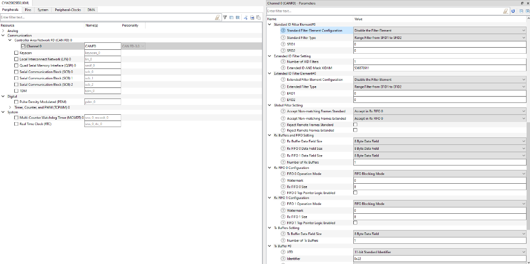
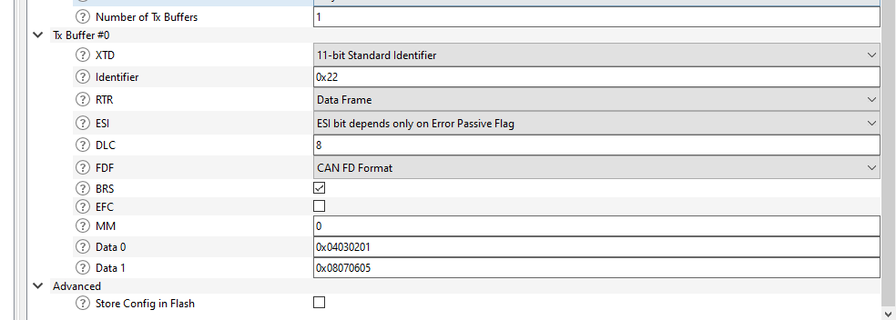
Applications and code example
CAN FD use cases are:
- Electronic Control Units (ECU)
- Industrial Automation
For example, the CAN FD code example demonstrates that CAN FD Node-1 sends a CAN FD frame to CAN FD Node-2 on pressing the user button and vice versa. Both the CAN FD nodes log the received data over the UART terminal. Each time a CAN FD frame is received, the user LED toggles.
Smart I/O
Smart I/O adds programmable logic to an I/O port. Smart I/O integrates Boolean logic functionality such as AND, OR, and XOR into a port. It also pre- or post-processes the signals between the high-speed I/O matrix (HSIOM) and the I/O port. For example, smart I/O can enable digital glue logic for input signals using multiple flip-flops without CPU intervention. HSIOM multiplexes GPIOs, sharing multiple functions, into peripheral devices selected by the user.
Features
- Integrate board-level Boolean logic functionality into a port
- Ability to pre-process HSIOM input signals from the GPIO port pins
- Ability to post-process HSIOM output signals to the GPIO port pins
- Supports all device power modes except Hibernate mode
- Integrate closely to the I/O pads, providing shortest signal paths with programmability
Description
This design consists of a PWM resource and a smart I/O resource, both creating square waves of slightly different frequencies. These square waves are routed through an exclusive-OR (XOR) gate within the smart I/O resource, yielding a signal with a gradually changing duty cycle. The rate of change is proportional to the difference between the output square wave frequencies. The signal is then output to IO1 of smart I/O port 9. Driving an LED with this signal results in a ramping effect, where the LED gradually gets brighter and dimmer alternately.
A 10 kHz clock drives the PWM with a period of 399 counts and a compare value of 200 counts. This provides a 50 percent duty cycle square wave with a 40 ms period. The smart I/O is clocked at 99 Hz using a divided clock sourced from CLK_PERI. This input clock is divided by four using the lookup tables (LUTs) of the smart I/O resource to produce a square wave with a 40.4 ms period.
To generate a square wave signal with a time period close to 40 ms, a 99 Hz clock is divided by four using a synchronous sequential circuit, which is realized using the LUTs of the smart I/O resource.
Block diagram
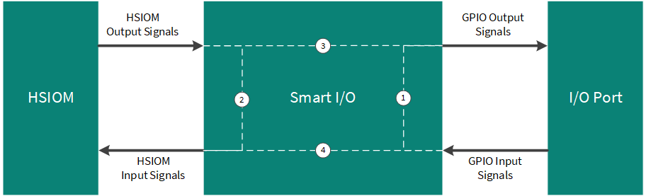
Block components
The internal logic of the smart I/O includes the following components:
- Clock and reset
- Synchronizers
- Three-input lookup table (LUT)
- Data unit (DU)
Clock and reset
The clock and reset component selects the smart I/O block’s clock (clk_block) and reset signal (rst_block_n). A single clock and reset signal is used for all components in the block. The clock and reset sources are determined by the CLOCK_SRC[4:0] bitfield of the SMARTIO_PRTx_CTL register. The selected clock is used for the synchronous logic in the block components, which includes the I/O input synchronizers, LUT, and data unit components. The selected reset is used to asynchronously reset the synchronous logic in the LUT and data unit components.
Note that the selected clock (clk_block) for the block’s synchronous logic is not phase-aligned with other synchronous logic in the device, operating on the same clock. Therefore, communication between smart I/O and other synchronous logic should be treated as asynchronous.
The following clock sources are available for selection:
- GPIO input signals “io_data_in[7:0]”. These clock sources have no associated reset
- HSIOM output signals “chip_data[7:0]”. These clock sources have no associated reset
- Smart I/O clock (clk_smartio). This is derived from the system clock (clk_sys) using a peripheral clock divider
- Low-frequency system clock (clk_lf). This clock is available in the System Deep Sleep power mode. This clock has an associated reset (rst_lf_dpslp_n). Reset is activated if the system enters Hibernate mode or is at POR
When the block is enabled, the selected clock (clk_block) and associated reset (rst_block_n) are provided to the fabric components. When the fabric is disabled, no clock is released to the fabric components and the reset is activated (the LUT and data unit components are set to the reset value of ‘0’). The I/O input synchronizers introduce a delay of two clk_block cycles (when synchronizers are enabled). As a result, in the first two cycles, the block may be exposed to stale data from the synchronizer output. Hence, during the first two clock cycles, the reset is activated and the block is in bypass mode.
Synchronizer
Each GPIO input signal and device input signal (HSIOM input) can be used either asynchronously or synchronously. To use the signals synchronously, a double flip-flop synchronizer (see Figure 52) is placed on both of these signal paths to synchronize the signal to the smart I/O clock (clk_block). The synchronization for each pin or input is enabled or disabled by setting or clearing the IO_SYNC_EN[i] bitfield for the GPIO input signal and CHIP_SYNC_EN[i] for the HSIOM signal in the SMARTIO_PRTx_SYNC_CTL register, where ‘i’ is the pin number.
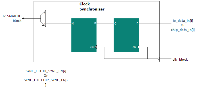
Lookup table (LUT)
Each LUT block takes three input signals and generates an output based on the configuration set in the SMARTIO_PRTx_LUT_CTLy register (y denotes the LUT number). For each LUT, an 8-bit lookup vector LUT[7:0] and a 2-bit opcode OPC[1:0] in the SMARTIO_PRTx_LUT_CTLy register determine the configuration. The 8-bit vector is used as a lookup table for the three input signals. The 2-bit opcode determines the use of the flip-flop. The LUT configuration for different opcodes is shown in Figure 53.
The SMARTIO_PRTx_LUT_SELy registers select the three input signals (tr0_in, tr1_in, and tr2_in) going into each LUT. The input can come from the following sources:
- Data unit output
- Other LUT output signals (tr_out)
- HSIOM output signals (chip_data[7:0])
- GPIO input signals (io_data[7:0])
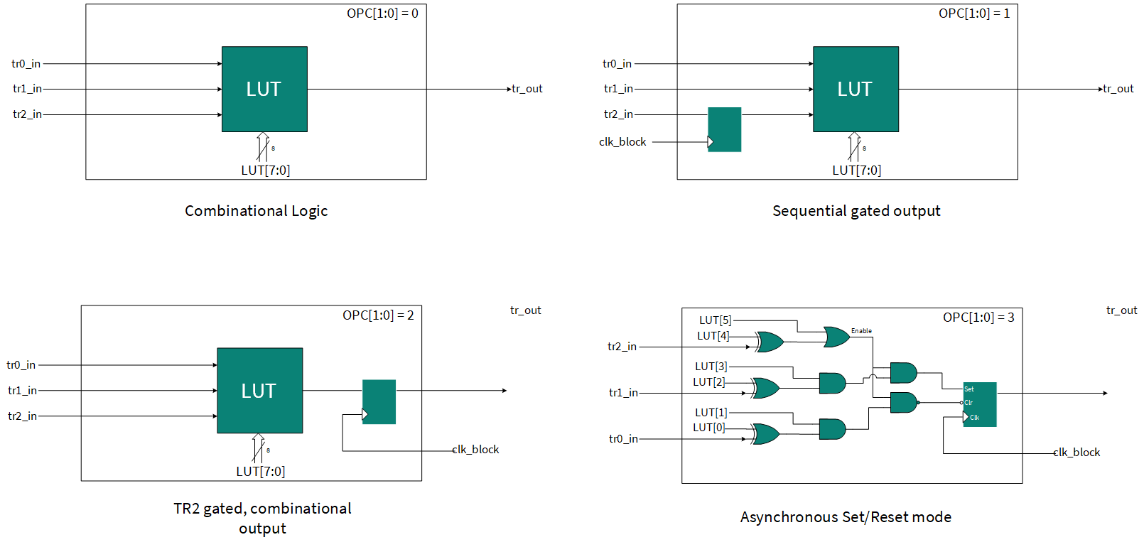
LUT has the following four operations selected by a 2-bit Op Code field (see Figure 53).
- Combinatorial LUT is purely combinatorial. Each LUT output is the result of the LUT mapping truth table and will only be delayed by the LUT3 [x] combinatorial path (basic mode)
- Gated Input LUT3 input 2 is registered. Other inputs are directly connected to LUT3 [x]. The output is combinatorial (input synchronization)
- Gated Output Inputs are directly connected to LUT3 [x], and the output is registered (output synchronization)
- Set/Reset flip-flop: Input signals are used to control an S/R flip-flop
Data unit (DU)
Each smart I/O block includes a data unit (DU) component. The DU consists of a simple 8-bit data path. It is capable of performing simple increment, decrement, increment/decrement, shift, and AND/OR operations. The operation performed by the DU is selected using a 4-bit opcode DU_OPC[3:0] bitfield in the SMARTIO_PRTx_DU_CTL register. The DU component supports up to three input trigger signals (tr0_in, tr1_in, and tr2_in), similar to the LUT component. These signals are used to initiate an operation defined by the DU opcode. In addition, the DU also includes two 8-bit data inputs (data0_in[7:0] and data1_in[7:0]) that are used to initialize the 8-bit internal state (data[7:0]) or to provide a reference. The 8-bit data input source is configured as:
- Constant ‘0x00’
- io_data_in[7:0]
- chip_data_in[7:0]
- DATA[7:0] bitfield of SMARTIO_PRTx_DATA register
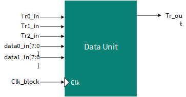
The trigger signals are selected using the DU_TRx_SEL[3:0] bitfield of the SMARTIO_PRTx_DU_SEL register. The DUT_-DATAx_SEL[1:0] bits of the SMARTIO_PRTx_DU_SEL register select the 8-bit input data source.
The DU_SIZE[2:0] bits of the SMARTIO_PRTx_DU_CTL register define the size of the DU (number of bits used by the data path). The DU generates a single output trigger signal (tr_out). The internal state (du_data[7:0]) is captured in flip-flops and requires clk_block.
Software usage
This section describes about the software usage of smart I/O using PDL API's and also explains the usage of Device configurator and smart I/O configurator.
For more details on the smart I/O PDL APIs, see Smart I/O PDL.
Smart I/O configuration flow
Do the following to configure and operate the smart I/O block:
- Before enabling the block, all the components and routing should be configured
- In addition to configuring the components and routing, some block level settings
must be configured correctly for desired operation
- Bypass control: To bypass the smart I/O path for a particular GPIO signal, set the BYPASS[i] bitfield in the SMARTIO_PRTx_CTL register. When bit ‘i’ is set in the BYPASS[7:0] bitfield, the ith GPIO signal is bypassed to the HSIOM signal path directly; smart I/O logic will not be present in that signal path. This is useful when the smart I/O function is required only on select I/Os
- Pipelined trigger mode: The LUT input multiplexers and the LUT component itself do not include any combinatorial loops. Similarly, the data unit also does not include any combinatorial loops. However, when one LUT interacts with the other or with the data unit, inadvertent combinatorial loops are possible. To overcome this limitation, the PIPELINE_EN bitfield of the SMARTIO_PRTx_CTL register is used. When set, all the outputs (LUT and DU) are registered before branching out to other components
- After the smart I/O block is configured for the desired functionality, set the ENABLED bitfield of the SMARTIO_PRTx_CTL register to enable the block. If disabled, the smart I/O block is put in bypass mode, where the GPIO signals are directly controlled by the HSIOM signals and vice versa. The smart I/O block must be configured; that is, all register settings must be updated before enabling the block to prevent glitches during register updates
Device Configurator
The smart I/O device configuration is configured in the ModusToolbox™ Software. The Device configurator is opened from the smart I/O project in ModusToolbox™ Software IDE. Figure 55 shows the smart I/O pin configuration in the PIN section.
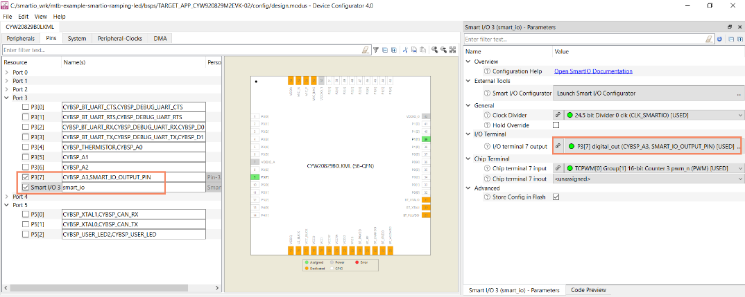
The PWM module provides the input for the smart I/O. The PWM is generated with the following configuration (see Figure 56): 50% Duty cycle.
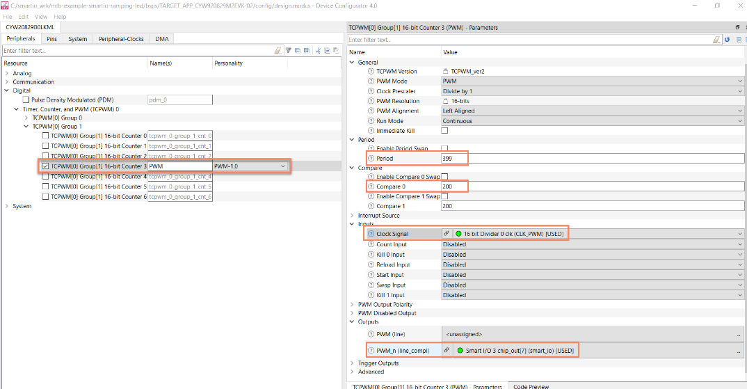
Clock configuration for smart I/O Frequency is set for 100 HZ.
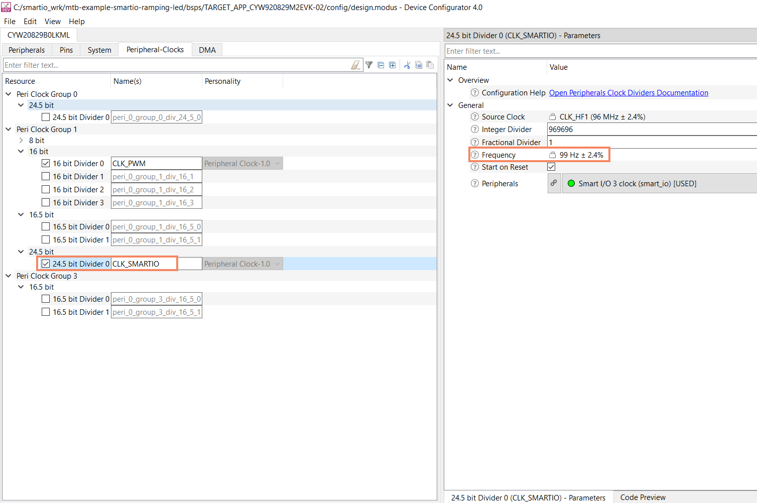
Clock configuration for PWM at 10-KHZ frequency.
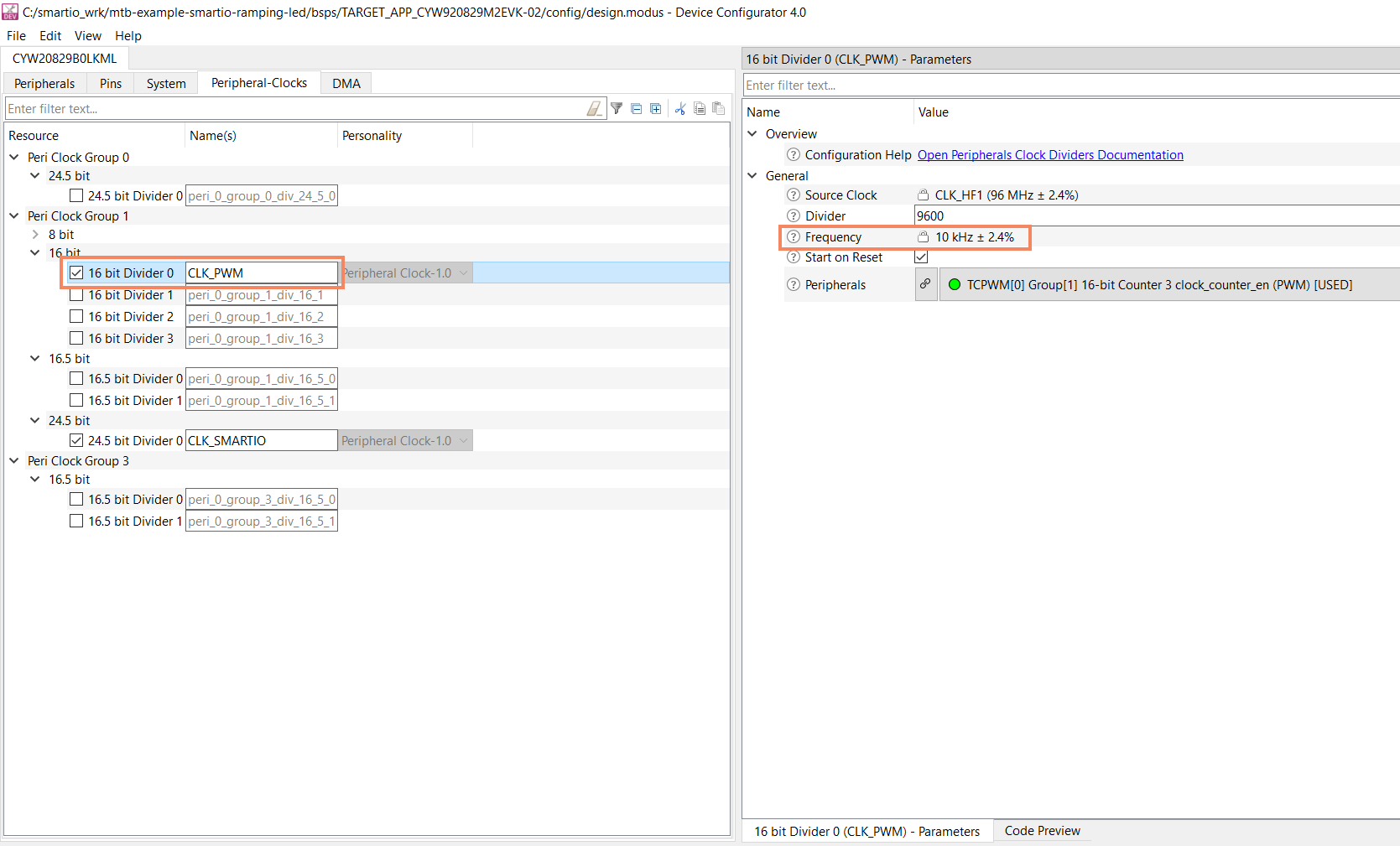
Opening smart I/O configurator can be opened in two ways. Directly from the project menu or from the device configurator. For more information, see ModusToolbox™ Smart I/O Configurator Guide.
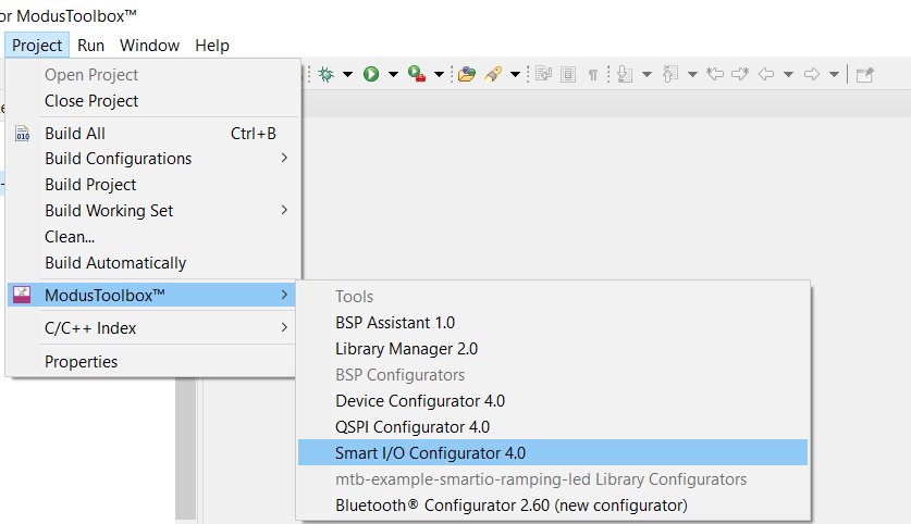
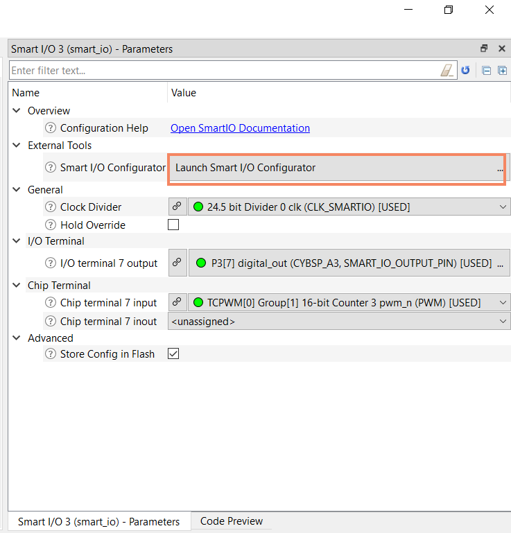
Routing the smart I/O
The smart I/O block includes many switches that are used to route the signals in and out of the block and also between various components present inside the block. The routing switches are handled through the PRTGIO_PRTx_LUT_SELy and SMARTIO_PRTx_DU_SEL registers. Figure 60 shows the smart I/O internal routing. In Figure 60, note that LUT7 to LUT4 operate on io_data/chip_data[7] to io_data/chip_data[4] whereas LUT3 to LUT0 operate on io_data/chip_data[3] to io_data/chip_data[0]. Figure 56 shows the smart I/O internal routing. Note that LUT7 to LUT4 operate on io_data/chip_data[7] to io_data/chip_data[4] whereas LUT3 to LUT0 operate on io_data/chip_data[3] to io_data/chip_data[0]. The “Ramping LED” uses the configuration shown in Figure 56.
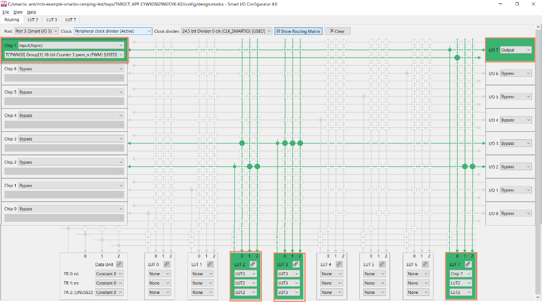
The following are the LUT operating modes and tables:
- Combinational output
Figure 61. Combinational output 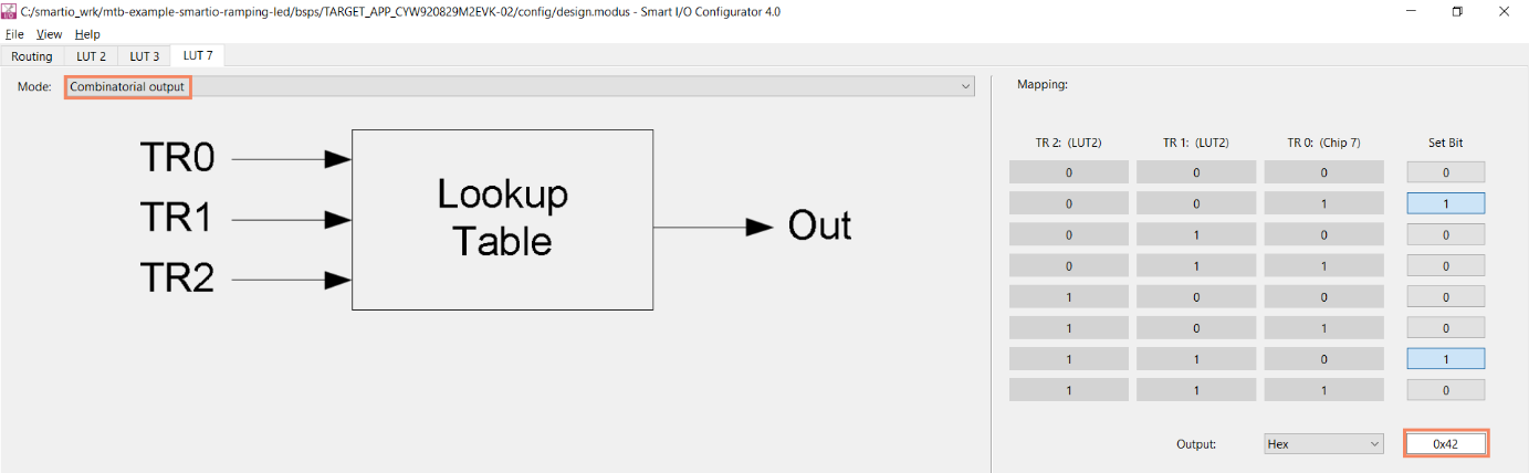
- Sequential (gated) output
Figure 62. Sequential (gated) output 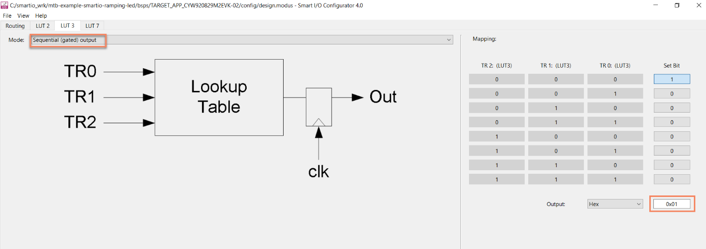
- TR2 gated, combinational output
Figure 63. TR2 gated, combinational output 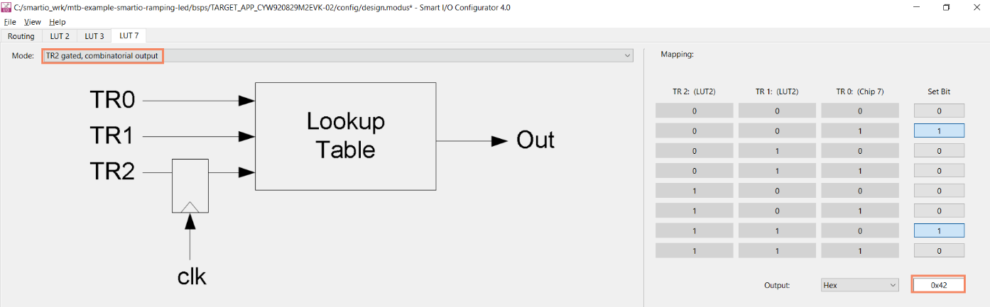
- Asynchronous Set/Reset mode
Figure 64. Asynchronous Set/Reset mode 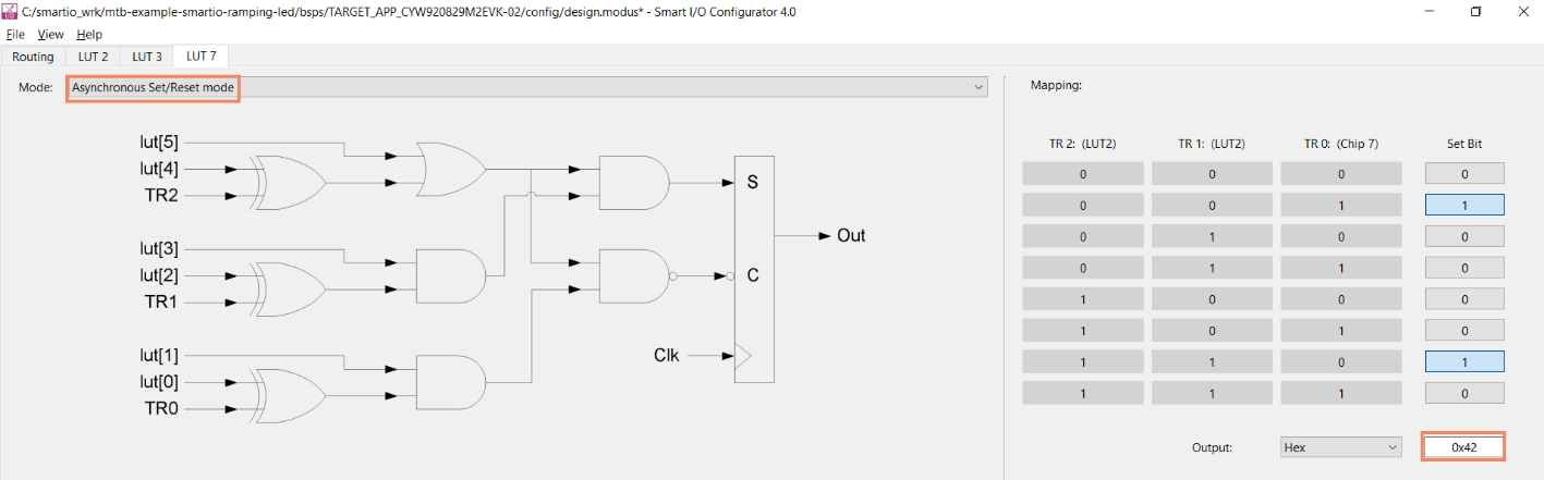
Applications and code examples
Use smart I/O to perform simple logic operations and routing on signals to or from the I/O pins.
Typical applications include the following:
- Change routing to or from pins: This function allows rerouting signals from the fixed-function peripherals to non-dedicated pins on the same port
- Invert the polarity of signal: This function inverts the polarity of output signals such as the SPI signal, before it goes out from a pin
- Clock or signal buffer: This function drives a GPIO input signal, which has to drive a heavier load for one pin, through two GPIO buffers
- Detect a pattern on pins: This function detects the patterns of several signal inputs and outputs the programmable signal depending on the result of detection
These applications of smart I/O can work in low-power mode (Deep Sleep), therefore can be used as a wakeup interrupt.
For example, see the Ramping LED using smart I/O code example.
Cryptolite
Introduction
The hardware-based cryptographic accelerator block is designed to speed up and efficiently carry out cryptographic functions. This hardware implementation uses less time compared to software implementation. One of the cryptographic functions accelerated by this block is the Advanced Encryption Standard (AES) functionality. AES includes a block cipher and an inverse block cipher. The block cipher encrypts a 128-bit block of plaintext data into a 128-bit block of ciphertext data, while the inverse block cipher decrypts a 128-bit block of ciphertext data into a 128-bit block of plaintext data using the same symmetric key.
The AES-128 block cipher function, a member of the AES block cipher family, provides message confidentiality and authenticity by encrypting each 128-bit block with a 128-bit key. The AES-128 block cipher function performs 10 rounds. During each round, a dedicated 128-bit round key is derived from the provided key, and the internal cipher state is updated.
It also offers support for SHA-256, a cryptographic hash function well-known for producing a uniform 256-bit (32-byte) hash value. This algorithm is a component of the esteemed secure hash algorithm family, developed by the National Security Agency (NSA) in the United States. Additionally, the True Random Number Generator (TRNG) component produces 32-bit true random numbers, ensuring a fixed bit size for the generated random values.
Features
The AES-128 hardware accelerator supports the following modes:
- Electronic Code Book (ECB) mode: Encryption is supported
- Cipher Block Chaining (CBC) mode: Encryption is supported
- Cipher Feedback (CFB) mode: Encryption and decryption are supported
- Counter (CTR) mode: Encryption and decryption are supported
- Output Feedback (OFB) mode: Not supported
The Secure Hash Algorithm (SHA) feature supports only SHA-256 to enhance hash functionality. Additionally, the True Random Number Generator (TRNG) component is based on a set of ring oscillators.
Description
Advanced encryption standard (AES)
AES is an iterative cipher that uses a substitution-permutation network to perform its encryption. Its process consists of interconnected operations, which involve either replacing inputs with specific outputs (substitutions) or rearranging bits (permutations). AES performs all its computations on bytes rather than bits. Thus, AES treats the 128 bits of a plaintext block as 16 bytes. These 16 bytes are arranged in four columns and four rows for processing as a matrix.
Encryption
There are four sub-processes involved in each round of AES. The initial round includes the following process:
- Byte substitution (SubBytes): During the initial round of AES, the 16 bytes of input are substituted by referencing a fixed table (S-box) that is pre-defined in the design. The output is then represented in the form of a 4x4 matrix, with four rows and four columns
- Shift rows: In the AES encryption process, each of the four rows of the matrix resulting from the substitution process is subjected to a left shift. The first row is not shifted at all. The second row is shifted one position to the left. The third row is shifted two positions to the left. The fourth row is shifted three positions to the left
- Mix columns: This process takes the four bytes of a single column as input and outputs four entirely new bytes, which are then used to replace the original column. This step is carried out in all rounds of AES, except for the last round
- Add round key: The 16 bytes of the matrix obtained from the column-mixing process are treated as a 128-bit value and subjected to an XOR operation with a 128-bit round key. If this is the last round of encryption, the resulting value represents the ciphertext. If it is not the last round, the resulting 128 bits are interpreted as 16 bytes, and the process is repeated for another round with a new round key
Decryption
To decrypt an AES ciphertext, the process is essentially the reverse of the encryption process. Each round of the decryption process involves performing the four operations in reverse order: Byte substitution, shift rows, mix columns, and add round key.
Secure hash algorithm (SHA)
The SHA-256 hash function, part of the SHA-2 hash family, operates by dividing a message into multiple 512-bit chunks and processing each chunk individually to calculate the message's hash value, also known as the message digest. It maintains an internal 256-bit hash state (comprising eight 32-bit words) denoted as H[j], where j = 0, …, 7. When processing the message chunks, the initial hash state for the first chunk is set to predetermined SHA-256 values. Subsequent message chunks begin with the previous chunk's concluding hash state, and the final hash state of the last message chunk represents the message's hash value.
The SHA-256 hash function executes 64 rounds of a compression function, with each round updating the internal hash state. Each round incorporates a dedicated 32-bit round constant K[i] and a specific 32-bit message schedule value W[i]. The round constants are fixed values pre-defined for SHA-256, while the message schedule values are derived from the 512-bit message chunk, making them specific to the message being processed.
True random number generator (TRNG)
The TRNG utilizes an array of up to six ring oscillators, each comprising a series of inverters connected in a feedback loop, to generate physical noise sources. The temperature-dependent variability of the inverter delays within each ring oscillator introduces random fluctuations, known as jitter, into the oscillating signal. This jittered signal is then digitized through sampling, resulting in a digitized analog signal (DAS) for each ring oscillator. This process is repeated across all ring oscillators, producing a collection of DAS outputs.
Software usage
This section describes the software usage of Cryptolite AES and SHA using PDL APIs and the device configurator. For additional documentation, see the following PDL APIs:
Sequence diagram
Device Configurator
Cryptolite is not supported in the Device Configurator.
Applications and code example
Some use cases for Cryptolite AES include:
- Encrypt data
- Decrypt data
Some use cases for Cryptolite SHA-256 include:
- Digital signatures
- Password storage
Some use cases for Cryptolite TRNG include:
- Secure communication
- Secure boot and firmware
CE239652 – Cryptolite is an example that demonstrates how to set up Cryptolite AES, SHA-256, and TRNG using the PDL resource. In this example, AES is used to perform encryption and decryption of data, SHA-256 is used to generate a message digest of the data, and TRNG is used to generate random numbers.
Interrupts
Introduction
Infineon's AIROC™ CYW20829, built around Cortex®-M33 cores, can handle both interrupts and CPU exceptions. In this context, any event that disrupts the normal flow of instruction execution is considered an exception by the CPU. This means that interrupt requests are also treated as exceptions.
There are two main types of events that can trigger an exception:
- Interrupts: These are generated by external peripherals such as timers, serial communication blocks, and port pin signals
- Exceptions: These are generated internally by the CPU, such as memory access faults and system timer events
When an exception occurs, the CPU stops executing the current program and instead executes the exception handler, or interrupt service routine (ISR).
Features
Infineon's AIROC™ CYW20829 supports the following interrupt features:
- Supports 70 system interrupts
- 70 Arm® Cortex®-M33 interrupts
- Up to 17 interrupt sources capable of waking the Cortex®-M33 from Deep Sleep power mode
- Each interrupt supports eight configurable priority levels on the Cortex®-M33
Description
When an interrupt or exception event is triggered, a specific sequence of events unfolds. Initially, the processor executes the main code, and all interrupt and exception signals are in an idle state. When a signal is triggered, the Nested Vectored Interrupt Controller (NVIC) detects the rising edge, registers the event, and places it in a pending state. The CPU then responds by storing its current context, pushing the contents of its registers onto the stack. Additionally, the CPU receives the unique exception number associated with the triggered interrupt from the NVIC. This exception number is used to fetch the address of the corresponding exception handler from the vector table. The CPU then branches to this address and executes the exception handler. Once the handler is complete, the CPU restores its registers to their original state using stack pop operations and resumes executing the main code.
In cases where multiple interrupts are triggered simultaneously or an interrupt is triggered while another is being serviced, the NVIC evaluates the priority of each interrupt and sends the exception number of the highest-priority interrupt to the CPU. This allows higher-priority interrupts to preempt lower-priority ones at any time. Exceptions are handled similarly, with each event having a unique exception number that the CPU uses to execute the appropriate exception handler.
There are different exception sources, including:
- Reset exception
- Non-maskable interrupt exception
- Hard fault exception
- Memory management fault exception
- Bus fault exception
- Usage fault exception
- Supervisor call exception
- Pend supervisory exception
- System tick exception
Software usage
For more information related to interrupts and their priority, see the GitHub page.
Applications and code example
Some use cases for interrupts include handling input/output operations, handling errors, and device driver events. An example is CE239178 – AIROC™ CYW20829 Bluetooth® LE SoC: Switching power modes. This example demonstrates how a button interrupt is handled.
Trigger multiplexer
Introduction
All peripherals within this MCU device are connected via trigger signals, which serve to indicate the occurrence of an event or a change in state. These triggers are used to activate or initiate operations in other peripherals. Trigger multiplexers facilitate the routing of triggers from a source peripheral to a destination, helping the user manage trigger pathways. Unlike interrupts, triggers are used for synchronization between peripherals rather than between a peripheral and the Arm® CPU core.
Features
The trigger multiplexer includes the following features:
- Ability to connect any trigger signal from one peripheral to another
- Provision of multiplexer-based trigger groups and one-to-one trigger groups
- Support for a software trigger that can activate any signal within the block
- Capability to configure the trigger multiplexer with hardware-based trigger manipulation features such as inversion and edge/level detection
- Ability to block triggers in debug mode
Description
Peripheral blocks generate digital signals known as triggers to indicate states, such as FIFO levels, or events, such as the completion of an action. These triggers serve as initiators for actions in other peripheral blocks. In this MCU, multiple peripheral blocks can be interconnected using trigger signals. To facilitate this, there is hardware called the trigger multiplexer block, which consists of a series of multiplexers used to route trigger signals from various sources to destinations.
The trigger multiplexer can receive trigger signals from any peripheral block and route them to initiate or affect operations in other peripheral blocks. There are two types of triggers: high-active, level-sensitive triggers and rising-edge, pulse triggers. The former reflects peripheral states and requires the consumer to deactivate the trigger, while the latter indicates the occurrence of an event.
A trigger component comprises multiple trigger groups, which can be of two types: one-to-one connectivity groups and multiplexer-based connectivity groups. The former connects a peripheral input trigger to a specific peripheral output trigger, while the latter connects a peripheral input trigger to multiple peripheral output triggers.
All input and output signals to a trigger multiplexer can be software-triggered by writing into the register, allowing the triggering of corresponding signals.
Software usage
This section explains the software usage of TrigMux (Trigger Multiplexer) using PDL APIs. For additional documentation, see TrigMux PDL API.
Sequence diagram
Device Configurator
To initialize the TriggerMUX, you can access the Device Configurator in ModusToolbox™ through various methods. One way is to right-click on the project, select ModusToolbox™, and then Device Configurator. Another option is to access it through the ModusToolbox™ Quick Panel located in the bottom-left corner of the window. In the Device Configurator, navigate to the peripheral section, choose the resource, and configure the trigger input and trigger output.
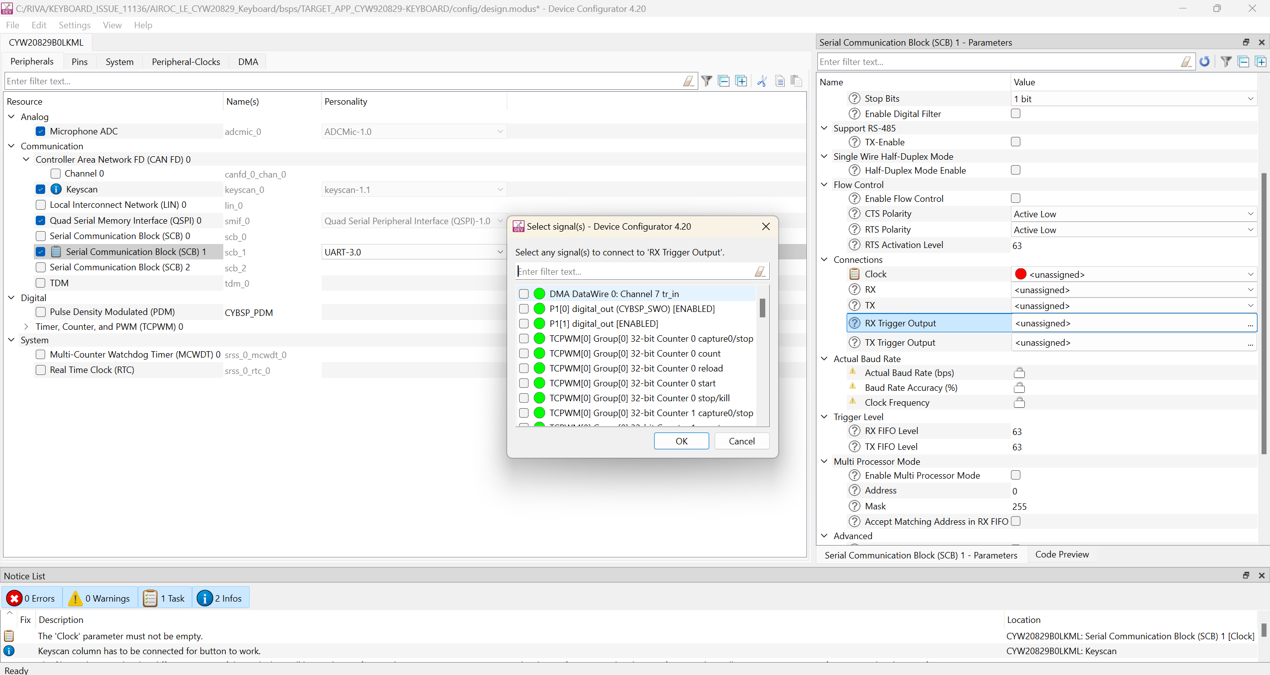
Applications
Some use cases for the Trigger Multiplexer include:
- Trigger selection and routing
- Software triggers
References
Application notes
- Infineon Technologies AG: 002-38254: Getting started with AIROC™ CYW20829 Bluetooth® LE on ModusToolbox™; Available online
User guides
- Infineon Technologies AG: 002-37529: CYW920829M2EVK-02 Evaluation Kit user guide; Available online
Release notes
- Infineon Technologies AG: 002-37478: CYW920829M2EVK-02 Evaluation Kit release notes; Available online
Revision history
| Document version | Date of release | Description of changes |
|---|---|---|
| ** | 2023-10-12 | Initial release |
| *A | 2024-01-31 | Removed “restricted” status Published to web |
| *B | 2024-04-04 | Updated template; no content update |
| *C | 2025-03-21 | Added the following sections: |
Trademarks
The Bluetooth® word mark and logos are registered trademarks owned by Bluetooth SIG, Inc., and any use of such marks by Infineon is under license.