About this document
Scope and purpose
AN238282 describes how to use the various power modes in AIROC™ CYW20829 Bluetooth® LE system-on-chip (SoC) for optimizing the power consumption based on the use cases. Major topics discussed in this application note include the power measurement procedure, low-power modes, tips for power saving, power management techniques, and sample applications available for CYW20829.
Intended audience
This application note is intended for users who are interested in minimizing the average power consumption of their respective Bluetooth® applications.
Introduction
AIROC™ CYW20829 is a high-performance, ultra-low-power and “Secure” MCU + Bluetooth® LE platform, purpose-built for IoT applications. It combines a high-performance microcontroller with Bluetooth® LE (5.4) connectivity, high-performance analog-to-digital conversion audio input, I2S/PCM, CAN, LIN for automotive use cases and other standard communication and timing peripherals. CYW20829 employs a high level of integration to minimize external components, reducing the device footprint and costs associated with implementing Bluetooth® Low Energy solutions. AIROC™ CYW20829 is the optimal solution for wireless input devices such as remotes, keyboards, joysticks, Bluetooth® Mesh, automotive, asset tracking, and other Bluetooth® LE IoT applications that need 10 dBm RF output power such as lighting and home automation. The AIROC™ CYW20829 Bluetooth® LE system-on-chip offers the best power-saving features and modes without significantly compromising the compute performance.
This application note requires the user to have basic knowledge about the AIROC™ CYW20829 architecture, and the ability to develop an AIROC™ CYW20829 application using ModusToolbox™ software. To get familiarized with the ModusToolbox™ environment, see the ModusToolbox™ user guide.
Infineon resources
Infineon provides a wealth of data at the www.infineon.com page to help you to select the right IoT device for your design, and quickly and effectively integrate the device into your design. Infineon provides customer access to a wide range of information, including technical documentation, schematic diagrams, product bill of materials, PCB layout information, and software updates. Customers can acquire technical documentation and software from the Infineon Developer Community.
ModusToolbox™
Infineon provides ModusToolbox™ as the software development platform for CYW208xx applications. ModusToolbox™ is a set of tools that enable you to integrate Infineon devices into your existing development methodology. One of the tools is a multi-platform, Eclipse IDE that supports application configuration and development. See .
Development kits
The CYW920829M2EVK-02 development kit enables you to evaluate Bluetooth® applications using AIROC™ CYW20829 Bluetooth® LE device. For more information on the kit and CYW20829, including the user guide and schematics, see the AIROC™ CYW20829 product information.
CYW20829 power architecture
Low-power system features
Clocks
CYW20829 power modes
CYW20829 can operate in the following system power modes. These modes are intended to minimize the average power consumption in an application.
The Arm® Cortex® M33 CPU core on CYW20829 can be operated in the following two voltage selection modes:
- System low power (LP) - All peripheral and CPU power modes are available at full speed with a regulated voltage of 1.1 V
- System ultra-low power (ULP) - All CPU peripherals and power modes are available but with limited speed and 1.0 V voltage regulation
CYW20829 has the following five SoC-level power modes:
- CPU Active: The CPU is executing code in system LP or ULP mode. The clock source to the CPU core can be chosen as minimum as 6 MHz to a maximum of 96 MHz
- CPU Sleep: CPU code execution is halted in system LP or ULP mode. The clock source to the CPU core is gated in this mode
- System Deep Sleep: Only low-frequency peripherals are available after MCU subsystem (MCUSS) and Bluetooth® subsystem (BTSS) CPUs enter CPU Deep Sleep mode
- System Deep Sleep RAM: Only the RAM and I/O states are retained. All system activity except for select low- power peripherals stop until the system exits this state. The CPU resets upon exit but can skip software initialization because the RAM contents are retained
- System Hibernate: Device and I/O states are frozen; the device resets on wakeup. Only Bluetooth® LE advertisements are possible on waking up from Hibernate mode
Figure 3 shows the power modes transitions in CYW20829.
System power mode transition of MCU and Bluetooth® subsystems
You can control the power mode switching at the MCU subsystem (MCUSS) level, but the Bluetooth® subsystem (BTSS) handles internally its own power modes state transition. For the device to enter a low-power mode such as Deep Sleep, both CPUs should be in Deep Sleep. Figure 4 shows the transition between different power modes from power-on reset (POR).
| Transition | Description | Transit triggers | Power mode |
|---|---|---|---|
|
1a |
MCUSS OFF to reset transition |
Power supply applied to CYW20829 |
Active |
|
1b |
Bluetooth® subsystem OFF to reset transition. It stays in reset until the MCUSS releases it |
Power supply applied to CYW20829 |
Active |
|
2 |
The MCUSS/Bluetooth® subsystem reset to Active mode transition. The Bluetooth® subsystem transition happens only after the MCUSS releases it from reset. Each subsystem can move between Active and Sleep modes independently |
Firmware (boot/startup) transitions from reset to Active mode. The MCUSS downloads configurations to the Bluetooth® subsystem (via inter-processor communication (IPC); both subsystems transition to Active mode |
Active |
|
3 |
The MCUSS moves to Deep Sleep; the Bluetooth® subsystem moves to Deep Sleep RAM state. The Deep Sleep and Deep Sleep RAM power modes do not make any difference in Bluetooth® subsystem operation |
Firmware (OS idle task) transitions from Active to Deep Sleep mode |
Deep Sleep |
|
4 |
Both MCUSS and Bluetooth® subsystem move to Deep Sleep RAM state |
Firmware (OS idle task) transitions from Active to Deep Sleep RAM mode |
Deep Sleep RAM |
|
5 |
The MCUSS moves from Deep Sleep to Active and resumes execution from where it entered Deep Sleep. The Bluetooth® subsystem moves to Active via the warm boot handler (Path 6) |
Deep Sleep wakeup sources |
Active |
|
6 |
Both MCUSS and Bluetooth® subsystem transition from Deep Sleep RAM to Active independently and execute the respective warm boot handler |
Deep Sleep wakeup sources |
Active |
|
7 |
The MCUSS initiates transition to Hibernate mode; the Bluetooth® subsystem cannot ignore this state. The device enters Hibernate mode |
Firmware transitions from Active to Hibernate mode |
Hibernate |
|
8 |
The MCUSS transitions from Hibernate to Active |
Hibernate wakeup sources |
Active |
|
9 |
The MCUSS releases the Bluetooth® subsystem from reset |
Bluetooth® LE stack initialization |
Active |
System power modes
CPU Active, Sleep, and Deep Sleep are standard Arm®- defined power modes supported by the Arm® CPU instruction set architecture (ISA). System LP, ULP, Deep Sleep, Deep Sleep RAM and Hibernate modes are additional low-power modes supported by CYW20829.
The CPU can be selectively placed in Sleep and Deep Sleep power modes as defined by Arm®. The CPU also implements a Deep Sleep RAM (DS-RAM) mode in which almost all the circuits except RAM are powered OFF. Data in RAM is retained to maintain the state. Upon exit, the CPU goes through a reset but can use the data in RAM to skip software initialization.
Table 2 gives more details for each power mode.
| Power mode | Description | SRAM | Available peripherals | Wakeup sources | Wakeup time | Boot | Reinit required |
|---|---|---|---|---|---|---|---|
|
Low-power Active |
All resources are available with maximum speed (up to 96 MHz) |
ON |
All peripherals |
NA |
NA |
NA |
No |
|
Ultra-low power Active |
All resources are available but at a lower speed (up to 48 MHz) |
ON |
All peripherals |
NA |
NA |
NA |
No |
|
CPU Sleep |
CPU halts the execution. The rest of the system is available |
ON |
All peripherals |
All peripherals |
NA |
Resume |
No |
|
Deep Sleep |
CPU halts execution. Most peripherals are turned OFF. High-frequency clocks are OFF. Low-frequency clocks available. SRAM memory is retained. Active mode retention registers are retained |
Retained |
1xSCB key scan RTC WDT/MCWDT |
GPIO SCB 0 WDT/MCWDT RTC key scan Bluetooth® LE event |
60 µs |
Resume |
No |
|
Deep Sleep RAM |
CPU halts execution. Most peripherals are in OFF state. High-frequency clocks are turned OFF. Low-frequency clocks are available. SRAM memory is retained. Active mode retention registers are not retained |
Retained |
1xSCB key scan RTC WDT/MCWDT |
GPIO SCB 0 WDT/MCWDT RTC key scan Bluetooth® LE event |
800 µs |
Warm boot |
Yes |
|
Hibernate |
CPUs and clocks are OFF. GPIO output states are frozen. RTC alarm and dedicated GPIO wakeup pins are available to wake up the system. Backup domain is available. SRAM is not retained |
OFF |
RTC WDT/MCWDT GPIO P0.5, P1.4 |
Hibernate pins ‘0’ and ‘1’ RTC WDT/MCWDT |
2000 µs |
Cold boot |
No |
System power mode selection in Device Configurator
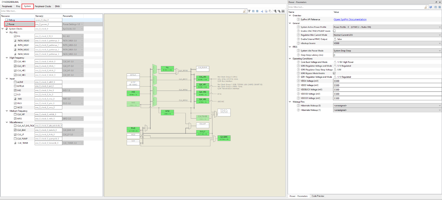
Device Configurator contains several tabs, each of which provides access to specific resources. Do the following:
- In the Project Explorer, right-click on the project and select
- Launch the Device Configurator for the selected application. See the Device Configurator user guide for more details
- Select the system to view the options for chip-wide configuration settings such as system clocks, power management, and debug interfaces
- Select the power subsection under System to view configurable power parameters available in CYW20829 as shown in Figure 5
| Sl. No | Parameter | Description | Range/options |
|---|---|---|---|
|
1 |
System Active Power Profile |
Selects the System Active power profile |
Options:
|
|
2 |
Regulator Min Current Mode |
Enables regulator minimum current mode |
Options:
|
|
3 |
System Idle Power Mode |
Selects the required power mode that the system stays in idle state |
Options:
|
|
4 |
hibernate_wakeup[ ] |
Reserves the hibernate_wakeup[0] pin to use it as the wakeup source from Hibernate power mode |
P0.5 (Fixed) |
|
5 |
hibernate_wakeup[1] |
Reserves the hibernate_wakeup[1] pin to use it as the wakeup source from Hibernate power mode |
P1.4 (Fixed) |
- Power Profile - 0 (LP MCU + Radio ON): All peripheral and CPU power modes are available with a maximum configurable CPU clock at 96 MHz with a regulated voltage of 1.1 V. Bluetooth® functionality is available because the radio module is powered ON
- Power Profile - 1 (ULP MCU + Radio ON): All CPU peripherals and power modes are available with the maximum frequency of 48 MHz and operating at 1.0 V voltage regulation (see Regulator operations). Bluetooth® functionality is available because the radio module is powered ON
- Power Profile - 2A (LP MCU Only): All peripheral and CPU power modes are available at full speed (96 MHz) with a regulated voltage of 1.1 V, but Bluetooth® functionality is not available because the radio module is in OFF state. The core buck voltage and mode are set to high power 1.16 V and SDR0 is set to regulated 1.1 V
- Power Profile – 2B (LP MCU Only): All peripheral and CPU power modes are available at full speed (96 MHz) with a regulated voltage of 1.1 V, but the Bluetooth® functionality is not available because the radio module is in OFF state. The core buck voltage and mode are set to low-power 1.1 V and SDR0 is set to bypassed 1.1 V
- Power Profile - 3 (ULP MCU Only): All CPU peripherals and power modes are available with the maximum frequency of 48 MHz and operating with a regulated voltage of 1.0 V. Bluetooth® radio module is turned OFF
- Regulator Min Current Mode: The user is responsible for ensuring that the
regulator current limit is met in their application. Two options are provided: (1)
Normal Current LDO (2) Minimum Current LDO
- Normal Current LDO: Sets the system to normal regulator current mode, which modifies system operation in LP or ULP modes to provide maximum core current consumption. If the LDO core regulator is in use, normal mode output current limits may be used. If the buck regulator is in use, its reduced current output limits still apply
- Minimum Current LDO: Sets the system to minimum core regulator current mode, which limits the maximum current available for the system core logic. This mode modifies system operation in LP or ULP modes to further reduce the current consumption. If the system current is below the datasheet current limits for the active core voltage regulator (LDO or buck), this mode may be entered
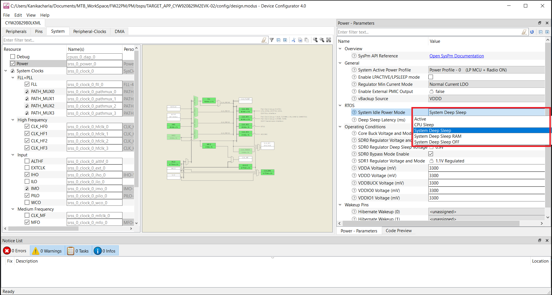
- System Idle Power Mode: The device stays in the selected idle power mode in idle state (for example, Active/Sleep/Deep Sleep/Deep Sleep RAM)
- Hibernate Wakeup: As the name suggests, wakeup pins are meant to wake up the device from Hibernate power mode. When the device wakes up from Hibernate, it goes through a cold boot procedure; see Boot
Device Configurator generates a set of macros as well as an initialization function using the options for regulators, peripherals, pins, clock sources, power modes, and profiles. All this functionality can also be done using the System Power Management (SysPm) library detailed below which can help you enable advanced use cases.
Power management by software
Boot
The boot procedure involves the initialization of various blocks of the CYW20829 SoC to get into basic operational mode before entering the application main() function. The boot procedure is invoked on POR, software reset, Hibernate wakeup, and Deep Sleep RAM wakeup.
CYW20829 supports two types of boot procedures depending on the power mode:
- Cold boot: POR, software reset and Hibernate wakeup will go through the cold boot procedure
- Warm boot: Deep Sleep RAM wakeup will go through the warm boot procedure
Cold boot
In this boot mode, system clocks and related clock paths are initialized and then the C runtime environment is set up before entering the main () function. For Hibernate wakeup, the device resets everything except the backup power domain resources. There is a small difference for initial power ON where even the backup power domain is reset. For more details on backup power domain, see Backup power domain.
Warm boot
Waking up from Deep Sleep RAM mode will result in a warm boot procedure. Warm boot is a shortened version of the complete boot process. The application can specify an entry point for warm boot, which is the starting point of execution for the CPU upon waking up from Deep Sleep RAM. This results in shortened boot procedure execution time.
This is done by using the Cy_Syslib_SetWarmBootEntryPoint() function. Using this function, an entry point such as a function address can be specified along with the stack pointer value that needs to be restored. See Implementing low-power mode transitions. This feature enables you to implement a variety of use cases such as the device can enter the Deep Sleep RAM state after setting an RTC alarm interrupt. When the alarm interrupt is triggered, the device wakes up from Deep Sleep RAM, the CPU executes the warm boot procedure, and the control is transferred to the entry point function.
Note that the warm boot procedure does not initialize the Serial Memory Interface (SMIF) block, so to jump to any function in the flash, the SMIF block must be initialized in the entry point function. Therefore, the entry point function is stored in the SRAM. To restore CPU execution from the point where it has entered low-power mode, the Cy_Syslib_SetWarmBootEntryPoint()function must be called immediately after wake- for- interrupt (WFI) and then the stack pointer restored. You can initialize the SMIF block and then jump to the main function depending on the use cases.
System Power Management (SysPm) library
PDL
The Peripheral Driver Library (PDL) is a complete software tool that includes APIs for configuring peripherals and system registers to implement the desired functionality. PDL provides direct access to almost all hardware resources of the target device. It reduces the need to understand and directly access registers and bit structures.
Within the PDL, the System Power Management (SysPm) API provides functions to change power
modes. The SysPm driver provides functions to register callback functions to execute before
or after power mode transitions as shown in Figure 6. The PDL is automatically downloaded when you create a new
application using the Project Creator tool. Alternatively, you can run the
make getlibs command from modus-shell. Note that this library has drivers
for subcategories 1A and 1B but CAT1B PDL drivers are supported only in CYW20829.
The SysPm PDL can be downloaded from ModusToolbox™ Peripheral Driver Library (mtb-pdl-cat1).
Callback modes
| Callback function | Description |
|---|---|
|
CY_SYSPM_CHECK_READY |
Checks the ready state to transition to other mode. Exits without transition if it returns CY_SYSPM_FAIL |
|
CY_SYSPM_CHECK_FAIL |
Callbacks execute only when CY_SYSPM_CHECK_READY fails. It executes the rollback action |
|
CY_SYSPM_BEFORE_TRANSITION |
Callbacks execute and configure required actions before mode transition |
|
CY_SYSPM_AFTER_DS_WFI_TRANSITION |
Performs the actions to be done after exiting Deep Sleep if entered and before interrupts are enabled |
|
CY_SYSPM_AFTER_TRANSITION |
Callbacks execute after mode transition or configuration |
The SysPm driver provides two functions for callback registration and execution. These functions not only help in power optimization, but also in preventing the peripheral from entering an undesired state after mode transition. When using PDL and HAL, you should register callbacks for each power mode. Most peripheral drivers have predefined callbacks associated with each power mode. You can choose to register the defined peripheral callback or can make a custom callback. The SysPm transition function executes the registered callbacks sequentially; the first registered function is executed first. For more information, see Register callback functions using PDL.
HAL
The Hardware Abstraction Layer (HAL) provides a high-level interface to configure and use hardware blocks on MCUs. It is a generic interface that can be used across multiple product families. The focus on ease-of-use and portability means that the HAL library does not expose all the low-level peripheral functionalities. Within the HAL, the system power management (SysPm) API provides functions to power management at the system level. This API can be used to perform functions such as setting Hibernate wakeup sources, setting the CPU power state, registering entry/wakeup callbacks, and entering system Sleep and Deep Sleep.
The HAL library is automatically downloaded when you create a new application using the Project Creator tool or you run the make getlibs command from modus-shell. It is recommended to use the HAL library as much as possible and move to the PDL library only when specific functionality is not available in the HAL library.
The SysPm HAL library can be downloaded from the ModusToolbox™ Hardware Abstraction Layer (mtb-hal-cat1) page.
Implementing low-power mode transitions
Implementing low-power modes on a bare metal application
The system can enter the following power modes such as Sleep, Deep Sleep, Deep Sleep RAM, and Hibernate using the HAL or PDL APIs. The following table lists the HAL APIs to switch between the different system power modes.
| Power mode | APIs |
|---|---|
|
Sleep |
cyhal_syspm_sleep() |
|
Deep Sleep |
cyhal_syspm_Deep Sleep() |
|
Deep Sleep RAM |
cyhal_syspm_Deep Sleep() |
|
Hibernate |
cyhal_syspm_hibernate() |
Because the same APIs are used to transition the device into Deep Sleep as well as Deep Sleep RAM, configure the idle power mode to transition CYW20829 into the respective modes. You can configure idle power mode by using Device Configurator (see Figure 7), or by changing it during runtime with the help of the Cy_SysPm_SetDeep SleepMode() API.
Steps to perform before entering Deep Sleep RAM mode
- Ensure that the warm boot entry point is set by using the
Cy_Syslib_SetWarmBootEntryPoint()function. To know more about warm boot entry, see Warm boot. - Register the Deep Sleep RAM callback with the priority set to ‘0’ to ‘9’ because the HAL SysPm callback priority is ‘10’.
- Note that upon waking up from Deep Sleep RAM, the system callback functions that have been registered by dependent software framework layers will be executed first, followed by the application-registered callback functions.
- Store NVIC registers to the RAM by using the
System_Store_NVIC_Reg()function to ensure that the NVIC register data is persistent after the device wakes up from Deep Sleep RAM.
Steps to perform after waking up from Deep Sleep RAM mode
- Enable all peripheral blocks through the peripheral control registers
and unfreeze all the I/Os by using the
SystemInit_Warmboot_CAT1B_CM33()function. - Initialize the SMIF block to use the flash.
- Restore the NVIC data from the RAM by using the
System_Restore_NVIC_Reg()function. - Execute the after-transition callback after exiting the low-power mode
by using the
Cy_SysPm_ExecuteCallback()function to perform the registered Deep Sleep RAM callbacks after wakeup. - In the registered Deep Sleep RAM callback, deinitialize and initialize the required peripherals.
The control will be redirected to other functions based on the application. The following code snippet showcases the process to be performed after waking up from DSRAM power mode.
| Waking up from Deep Sleep RAM mode |
|---|
/* DS-RAM Warmboot Re-entry */ cy_stc_syspm_warmboot_entrypoint_t syspm_app_dsram_entry_point = {(uint32_t *)&__INITIAL_SP, (uint32_t *)cy_app_warmboot_handler}; CY_SECTION_RAMFUNC_BEGIN int cy_app_warmboot_handler(void) { warm_boot=1; SystemInit_Warmboot_CAT1B_CM33(); cybsp_smif_init(); init_cycfg_all(); System_Restore_NVIC_Reg(); /* Suppress a compiler warning about unused return value */ (void)Cy_SysPm_ExecuteCallback(((cy_en_syspm_callback_type_t) CY_SYSPM_DEEP SLEEP_RAM), CY_SYSPM_AFTER_TRANSITION); main(); return 0; } CY_SECTION_RAMFUNC_END cy_rslt_t cybsp_syspm_dsram_init(void) { /* Sets the warm boot entry point and disables the debug pins */ Cy_Syslib_SetWarmBootEntryPoint((uint32_t*)&syspm_app_dsram_entry_point, false); return CY_RSLT_SUCCESS; } |
Implementing low-power modes on FreeRTOS
The idle power mode determines all power mode transitions in FreeRTOS as shown in Figure 7. When idle power mode is configured as Deep Sleep RAM, a FreeRTOS framework is created in such a way that it can do the following:
- Store the current context of the idle task
- Set the warm boot entry point
- Store and re-store NVIC registers to/from the RAM
- Execute the after-transition callback handler
Steps to perform before entering Deep Sleep RAM
- Ensure that debug mode is disabled by passing the second parameter as
‘false’ to the
Cy_Syslib_SetWarmBootEntryPoint()function. - When idle power mode is set to Deep Sleep, to enter Deep Sleep RAM at runtime, change
the idle power mode at runtime by adding the following code
block:
Cy_SysPm_SetDeep SleepMode(CY_SYSPM_MODE_DEEP SLEEP_RAM); - Add the Deep Sleep RAM latency by adding the following configuration in the application
Makefile:
# Add additional defines to the build process (without a leading -D).
DEFINES+=CY_CFG_PWR_DEEP SLEEP_RAM_LATENCY=20
Steps to perform after waking up from Deep Sleep RAM
Re-initialize the required peripherals in the after-transition callback.
See RTOS tickless mode for more information of power transition in RTOS.
Cy_Syslib_SetWarmBootEntryPoint() function. Register callback functions using PDL
The below code snippet showcases how to register the SysPm callbacks.
| Registering system power mode callbacks |
|---|
cy_stc_syspm_callback_params_t syspm_cpu_sleep_params; cy_stc_syspm_callback_params_t syspm_deep_sleep_params; cy_stc_syspm_callback_params_t syspm_hibernate_params; cy_stc_syspm_callback_params_t syspm_dsram_params; cy_stc_syspm_callback_t syspm_cpu_sleep_cb_handler = { syspm_cpu_sleep_cb, CY_SYSPM_SLEEP, 0u, &syspm_cpu_sleep_params, NULL, NULL, 253 }; cy_stc_syspm_callback_t syspm_deep_sleep_cb_handler = { syspm_ds_cb, CY_SYSPM_DEEP SLEEP, 0u, &syspm_deep_sleep_params, NULL, NULL, 253 }; cy_stc_syspm_callback_t syspm_dsram_cb_handler = { syspm_dsram_cb, CY_SYSPM_DEEP SLEEP_RAM, 0u, &syspm_dsram_params, NULL, NULL, 0 }; cy_stc_syspm_callback_t syspm_hibernate_handler = { syspm_hibernate_cb, CY_SYSPM_HIBERNATE, 0u, &syspm_hibernate_params, NULL, NULL, 253 }; Cy_SysPm_RegisterCallback(&syspm_cpu_sleep_cb_handler); Cy_SysPm_RegisterCallback(&syspm_deep_sleep_cb_handler); Cy_SysPm_RegisterCallback(&syspm_dsram_cb_handler); Cy_SysPm_RegisterCallback(&syspm_hibernate_handler); |
Implement custom callback functions using PDL
In the SysPm callback, you can define the actions to be performed before and after the power mode transition. For example, the following code snippet sets the CTS and RTS GPIOs to High-Z before entering Deep Sleep RAM mode and sets these GPIOs to the default pull-up configuration after wakeup.
| Implementing user defined SysPm callback |
|---|
|
Tips for active power saving
Use CYW20829 to gate current paths
The board may contain other components that draw power; therefore, you need to isolate the components that may draw current when not in use. GPIOs can source and sink higher currents to various components such as temperature sensors and digital mic. These GPIOs can be used to directly power some external peripherals (if the sensor requires within the GPIO supported current limit). The power to the external peripherals can then be directly controlled through the CYW20829 device; when not required, the peripherals can be turned OFF, so saving power at the system level.
GPIO configuration
GPIOs can hold their logic states in low-power modes. This is helpful when you need to hold external logic at a fixed level, but it can lead to wasted power if the pins needlessly source or sink current. The specific power saving of this technique depends on the circuit attached to the specific GPIO pin.
Analyze your design and determine the best state for your GPIOs during low-power operation.
cyhal_gpio_write()./* Set P0_0 to ‘0’ for low power using HAL APIs */ cyhal_gpio_write(P0_0,0u);
Configure all unused GPIOs to Analog High-Z unless there is a specific reason to use a different drive mode.
The Analog High-Impedance drive mode results in the lowest current for a GPIO pin. A pin’s
drive mode may be set using the cyhal_gpio_configure() HAL function.
/* Set P0_0 to Analog HI-Z for low power using HAL APIs. */
    cyhal_gpio_configure(P0_0, CYHAL_GPIO_DIR_INPUT, CYHAL_GPIO_DRIVE_ANALOG);
Clock gating
Some clocks and peripherals can be disabled when they are not necessary.
Unused clock sources: The System Resources subsystem provides many internal clock sources. Clock sources that are not utilized by any peripheral blocks can be disabled. Note that some clock sources, such as the crystal oscillators (WCO) have relatively long startup times. Switching these circuits OFF and ON may result in more overall current.
Frequency can be reduced by either selecting a low-frequency source such as IMO or selecting a different output frequency (for example, FLL) or dividing the clock using the System Resources subsystem Predividers or PERI dividers.
Use DMA to copy/move data
Direct memory access (DMA) is a technique that enables data transfer to and from the memory without involving the CPU. By bypassing the CPU, DMA can significantly reduce CPU utilization and power consumption. DMA can read and write data in blocks, which reduces the number of memory accesses required and saves power. Additionally, DMA can transfer data in bursts, which improves bus utilization and reduces power consumption. DMA can perform data transfers simultaneously with CPU processing, reducing the latency and power consumption of a system. DMA can also eliminate wait states, which occur when the CPU has to wait for a slow device to complete a data transfer, thereby saving power.
Furthermore, DMA can reduce the number of interrupts generated by a system, which in turn reduces both the CPU utilization and power consumption. DMA can operate at a lower clock frequency than the CPU, resulting in reduced power consumption. Lastly, the DMA engine can be used in both system LP and ULP modes, allowing data to be transferred without the use of the CPU. Overall, DMA offers several ways to reduce power consumption in a system by minimizing the interaction between the CPU and peripherals.
Audio subsystem
The I2S (TDM) and PDM/PCM blocks are generally sourced by a high-frequency clock generated from the PLL. If the audio subsystem is not in use, disable the I2S and/or PDM/PCM blocks. Also disable the FLL, which is the main reason for high current consumption. If the accuracy of the frame rates is not important for the application, do not use the FLL. Instead of using audio subsystem interrupts to access its FIFO in firmware, use DMAs controlled by the FIFO-level triggers to reduce the number of CPU cycles required in the application so that the CPU can stay in a Sleep state longer or execute other tasks.
Periodic wakeup timers
A periodic wakeup from CPU Sleep mode is the most common way to reduce power consumption. The average power consumption is determined by the ratio of CPU Active period power consumption and CPU Sleep period power consumption.
SRAM
CYW20829 allows powering OFF individual SRAM banks or pages within a bank. The size of pages within a bank depends on the specific device and bank as detailed in the device datasheet. Specific devices will have one or more SRAM banks. Any unused page can be disabled by writing to the CPUSS power control registers. This technique is most useful in System Deep Sleep mode in which retaining 128 KB SRAM consumes 5 µA and while retaining 256 KB SRAM consumes 6 µA of operational current as mentioned in the datasheet.
The CYW20829 SRAM consists of 256 KB of memory; it is further divided into four pages as shown in Figure 9. Each page can be powered OFF individually by using the following code snippet; to do so, make sure that the respective page does not hold any data.
The following changes need to be done in the application to power OFF the SRAM Bank 0:
- Update the linker script in the linker_ns_flash.ld file to prevent that data from being
placed in SRAM Bank
0:
RAM_START_ADDR_SAHB         = 0x20010000;
RAM_START_ADDR_CBUS         = 0x20010000;
- Update the size of the SRAM in the bsp.mk file:
DEVICE_CYW20829B0LKML_SRAM_KB=192
- Use the following function to power OFF SRAM Bank
0:
/* To power OFF the certain RAM section */
Cy_SysPm_SetSRAMMacroPwrMode(CY_SYSPM_SRAM0_MEMORY,0,CY_SYSPM_SRAM_PWR_MODE_OFF);
SCB
Avoid using blocking functions when sending or receiving data. Use interrupt-based events or an RTOS to transfer the data while yielding the CPU to other tasks. The idea behind this strategy is to keep the CPU in a Sleep state longer, instead of polling the status of the transmission. Figure 10 shows an example of blocking and non-blocking functions.
Instead of using the SCB interrupt to access its FIFO in firmware, use DMAs controlled by the FIFO level to reduce the number of CPU cycles required in the application. This helps the CPU to stay in the Sleep state longer to reduce the power consumption, or it can execute other tasks. One of the SCBs in CYW20829 is available in Deep Sleep mode. This feature can be used to keep the system in Deep Sleep mode while waiting for serial communication data from an external device.
TCPWM
When using a counter, timer, or PWM, you should configure the clock sourcing the channel as low as possible while still meeting your frequency and accuracy requirements. For example, if you need to generate a 1-second interrupt with a timer, it is better to use a clock frequency of 1 kHz with the period equaling 1,000 counts than a clock frequency of 1 MHz with a period equal to 1,000,000 counts. The power savings from reducing the TCPWM clock is mostly linear based on the clock frequency.
The same idea applies when using a PWM to dim an LED. Use the minimum clock frequency possible that does not let the human eye perceive that the LED is blinking. 60 Hz is a good frequency for most applications. A comparison between the clock settings for the TCPWM block is shown in Figure 11.
The TCPWM block has a clock prescaler feature. For minimum power consumption, maximize the peripheral clock divider first before using the TCPWM Clock Prescaler. If the TCPWM block uses any pin connections, set the pins to Analog High-Z when the block is disabled.
RTOS tickless mode
All RTOS require a clock or a ‘tick’ for timing and managing tasks. These ticks are usually small RTOS kernel tasks that wake up periodically and update the RTOS tick count used by delays, timeouts, and other timing-related tasks. Often, these ticks are configured in ms. This results in the CPU waking up often just to service the tick task even if it is not running any useful tasks.
Applications that do not use delays or timeouts or use large delays need not wake up this often and can enter a tickless mode provided by the platform. In tickless mode, the RTOS suspends the tick task and lets the CPU enter a low-power state (Deep Sleep) for longer durations. This duration is typically determined by the time the next task that depends on a delay needs to be triggered. If there are no tasks dependent on delays, the device can remain in the low-power state indefinitely until an external event (such as a GPIO interrupt) wakes up the device and triggers the task.
When delays are involved while entering tickless mode, a timer that is active in the system Deep Sleep state is configured to generate an interrupt after the delay expires.
All RTOS platforms provide a tickless mode of operation. In addition, you can control whether the OS enters Sleep or Deep Sleep when idle. This is useful when the OS (CPU) can be idle but peripherals such as an ADC or UART still operate and require the system to not enter Deep Sleep. You can ‘lock’ Deep Sleep entry in such cases, allowing the CPU to enter Sleep instead and ‘unlock’ the Deep Sleep entry after the peripheral completes its operation.
Advanced power management
Power control architecture
CYW20829 uses the Arm® power control architecture. The components used to control a single power domain are shown in Figure 12.
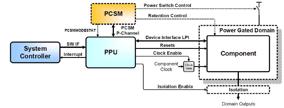
- Power Policy Unit (PPU) usually controls a power domain, but it can also be used to implement separate reset domains within a single power domain. The “SW IF” is the software interface from the system controller (for example, M33 processor). It is an Advanced Peripheral Bus (APB) interface at the PPU, and it is mapped to the Advanced High-performance Bus (AHB) memory-mapped I/O (MMIO) through an asynchronous bus bridge. The interface labeled “LPI” stands for Low Power Interface, which is usually implemented as a Q- or P-channel
- Power Control State Machine (PCSM) is a custom hardware module that controls the power switches. System Controller refers to an MCU (for example, M33). For the specific case of the main active PPU that controls VCCACT_PD, the system controller is inside the power-gated domain. In this case, the software interface (SW IF) and Interrupt signals are isolated as required
There is one more custom component called “Power Dependency Control Matrix (PDCM)” that is present in Arm® reference design. All PPUs interface with the PDCM, which handles dependency relationships between power domains.
Power states supported by each PPU
CYW20829 has three PPUs. See Table 6 and Table 7.
| PPU | PPU state |
|---|---|
|
PPU_MAIN |
FULL_RETENTION |
|
MEMORY_RETENTION |
|
|
OFF |
|
|
ON |
|
|
PPU_CPUSS |
FULL_RETENTION |
|
OFF |
|
|
ON |
|
|
PPU_SRAM |
MEMORY_RETENTION |
|
OFF |
|
|
ON |
| Deep Sleep state | PPU power modes |
|---|---|
|
Deep Sleep |
PPU_MAIN: FULL_RETENTION |
|
PPU_CPUSS: FULL_RETENTION |
|
|
PPU_SRAM: MEMORY_RETENTION |
|
|
Deep Sleep RAM |
PPU_MAIN: MEMORY_RETENTION |
|
PPU_CPUSS: OFF |
|
|
PPU_SRAM: MEMORY_RETENTION |
Regulator topologies
The regulator block in CYW20829 is a switching boot regulator with linear, step-down regulators. This topology uses the core buck switching regulator (CBUCK) after a transition from OFF or XRES. The CBUCK target voltage is programmable.
Two linear stepdown regulators (SDR0 and SDR1) generate core rails for system usage:
- SDR0 generates VCCD, which is the CPU core voltage
- SDR1 is for general usage. It can be used as either for an independent digital domain or as a regulator for the Bluetooth® LE radio
Core voltage selection
Linear regulator and buck regulator
- Core buck regulator (CBUCK): This regulator can either directly generate VCCD, or it can generate an intermediate voltage (VCCI) for use by step-down regulators. When the device is in Deep Sleep, the VCCD voltage will be changed to 0.9 V
- Linear step-down regulators (SDR0 and SDR1): Each SDR is a linear LDO regulator that uses VCCI to generate a low-voltage core supply rail (for example, VCCD). Both CBUCK modes (low-power and low-ripple) work with the SDRs target the platform voltage levels (1.0 V and 1.1 V) with either sufficient headroom for the SDR to work or in bypass mode. SDR0 can be bypassed when the input voltage is too low for regulation and is within the timing closure of the connected logic
- HV-LDO: This is a linear low drop-out regulator that uses VDDD to generate a programmable voltage
Assignment of regulators
- SDR0 is assigned to be the digital step-down regulator
- SDR1 is assigned to be the RF step-down regulator (RF-SDR) for use by the Bluetooth® subsystem. During Deep Sleep, this SDR is disabled
- HV-LDO is assigned to be the PA-LDO to supply the power amplifier in the radio for 10 dBm transmit case
Regulator operations
- CBUCK: This regulator operates in low-ripple and low-power modes. Low-ripple mode is used when the radio is operating
- SDR0 (D-SDR): This regulator operates in bypass or regulation mode, depending on the configuration and input voltage. This allows the CBUCK regulator to directly target the digital voltage, which improves overall power efficiency when the digital system is operating but the radio is not. It is expected to operate in bypass and regulation modes using CBUCK low-power or low-ripple modes. The SDR0 voltage can be changed through Device Configurator by selecting the System Active profile to ULP. This can also be changed it at runtime by using the following code snippet:
| Configuring the SDR0 voltage configurations |
#define CY_CFG_PWR_SDR0_VOLT CY_SYSPM_SDR_VOLTAGE_1_000V static cy_stc_syspm_sdr_params_t sdr0ConfigParam = { .coreBuckVoltSel = CY_CFG_PWR_CBUCK_VOLT, .coreBuckMode = CY_CFG_PWR_CBUCK_MODE, .coreBuckDpSlpVoltSel = CY_SYSPM_CORE_BUCK_VOLTAGE_0_90V, .coreBuckDpSlpMode = CY_SYSPM_CORE_BUCK_MODE_LP, .sdr0DpSlpVoltSel = CY_SYSPM_SDR_VOLTAGE_0_900V, .sdrVoltSel = CY_CFG_PWR_SDR0_VOLT, .sdr0Allowbypass = CY_CFG_PWR_SDR0_MODE_BYPASS, }; /* SDR0 Regulator Configuration */ Cy_SysPm_SdrConfigure(CY_SYSPM_SDR_0, &sdr0ConfigParam); |
- SDR1 (RF-SDR): This regulator supplies the power to the radio, and it can assume the CBUCK operates in low-ripple mode above the intended output voltage. It is not expected to operate in bypass mode using the CBUCK low-ripple mode
Backup power domain
The backup power domain contains the following major components:
- Backup clock
- ILO
- WCO
- PILO
- Real-time clock (RTC)
- Backup registers (BREG) to hold a small amount of application state
The backup domain contains the logic that can survive most resets, including XRES. The backup domain supply pin (VBACKUP) can be entirely independent from VDDD, and it can continue running when VDDD is not present. VBACKUP should be connected to the always-available power supply source to maximize features and compatibility with low-power modes. This can be an independent supply derived from a battery or super capacitor.
Backup data registers
The backup domain includes sixteen 32-bit registers, BACKUP_BREG[15:0], that retain their contents as long as the VBACKUP supply is valid. Each register holds 4 bytes of data for a total of 64 bytes. These registers are used to retain important system information and flags during power down of the full device. They can also be used during system Hibernate mode, allowing data to be read after device wake and reset. This can be used by the user to store some data in the backup domain so that it is retained even in case of power failures in the main supply. The handling of the backup registers is taken care of by the low-level driver APIs; the user application does not have any need to control these registers.
Low-power code examples
CE237951 – AIROC™ CYW20829 switching power modes
This code example shows how to transition the device to low-power and ultra-low-power system, and transition from Active to Sleep, Active to Deep Sleep, Active to Deep Sleep RAM, and Active to Hibernate power modes.
The code example uses a user button to change the power modes from Active to Sleep, Active to Deep Sleep, Active to Deep Sleep RAM and Active to Hibernate. After the system enters Hibernate mode, it waits for the wakeup resource. Another user button changes the power system from low-power and ultra-low-power system and vice versa. This code example shows User button 1 as a wakeup resource. Figure 14 shows the state machine implemented in the firmware to execute the transitions.
CE238052 – AIROC™ CYW20829 FreeRTOS switching power modes
This code example shows how to transition the device from Active to Sleep, Active to Deep Sleep, Active to Deep Sleep RAM, and Active to Hibernate power modes.
The code example uses User button 1 to change the power modes from Active to Sleep, Active to Deep Sleep, Active to Deep Sleep RAM, and Active to Hibernate. After the system enters Hibernate mode, it waits for the wakeup resource. This code example shows User button 1 as a wakeup resource. Figure 15 shows the state machine implemented in the firmware to execute the transitions.
CE237278 – HAL RTC alarm periodic wakeup
This code example shows how to enter Deep Sleep and Hibernate modes, as well as how to use the RTC to generate an RTC alarm to wake up the MCUSS from Deep Sleep and Hibernate modes.
The MCUSS enters either Deep Sleep or Hibernate mode based on the duration that the user button is pressed. The RTC alarm wakes up the system and prints the wakeup information to the UART terminal. Figure 16 shows the state machine implemented in the firmware to execute the transitions. For more information, see CE237278 - HAL RTC alarm periodic wakeup.
Power measurement
Hardware
- To measure the current consumed by the VIO_BASE domain, connect an ammeter across pins 1 and 2 of jumper J17, which is VDDIO. In CYW920829M2EVK-02, the external flash is connected to VDDIO and a voltage regulator; therefore, the measured current on VDDIO may depend on the selected external serial flash and voltage regulator
- To measure the current consumed by the VBAT domain, connect an ammeter across J9.3 and one of the pins J9.1, J9.4, J9.5 based on the power supply chosen
- To measure the current consumed by the VDDPA domain, connect an ammeter across J12.3 and one of the pins J12.1, J12.4, J12.5 based on the power supply chosen
- To measure the VCCD voltage, connect a voltmeter across TP1 with respect to GND. This is useful for finding whether the device has entered Deep Sleep. When the device enters Deep Sleep, the voltage across TP1 will be 0.9 V. When the CPU is in ULP mode and LP mode, the voltage across TP1 will be 1.0 V and 1.1 V respectively
Average current consumption
This section describes the average current consumption in low-power modes. The current is measured in each low-power mode for a certain period to calculate the average current consumption. The Active mode power consumption varies depending on various factors including the number of peripherals active and the operating clock frequency.
The connection interval preferred by the Bluetooth® LE GAP central device is used to establish the connection with the Bluetooth® LE GAP peripheral. Other values might be requested by the GAP peripheral device, but the GAP central device is still in charge of determining the connection parameters.
The connection interval and peripheral latency must be chosen optimally while trading off between power consumption and data throughput. For example, a longer connection interval (such as 4 seconds) will reduce the power usage but decrease the throughput. Therefore, you can increase the data throughput by lowering the connection interval value, but bear in mind that doing so will also result in an increase in power consumption.
On some peripheral devices, the Bluetooth® LE stack may let you select a minimum and maximum connection interval. Instead of selecting a value that is different from the minimum and perhaps beyond the permissible range for the peripheral device, the central can choose an acceptable value within the range using the maximum connection interval value that is provided by the peripheral.
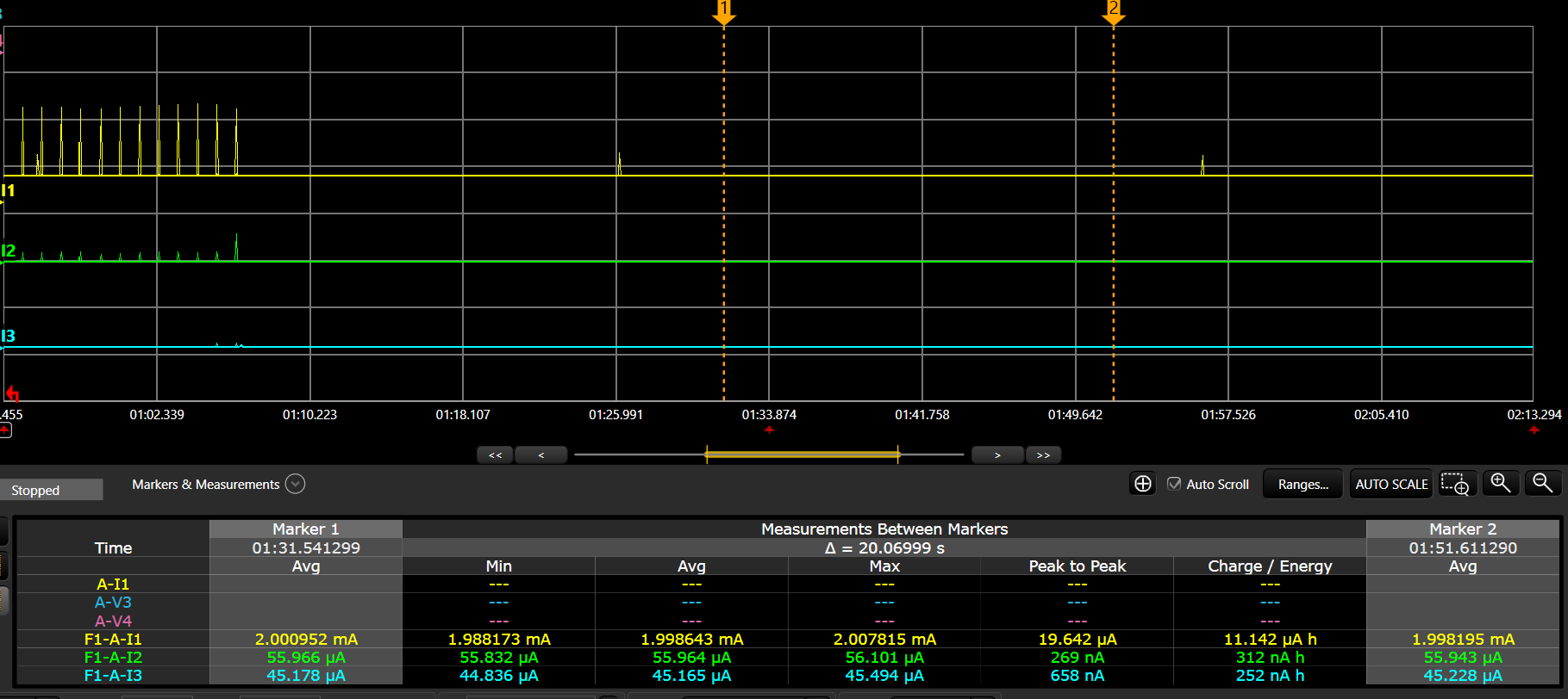
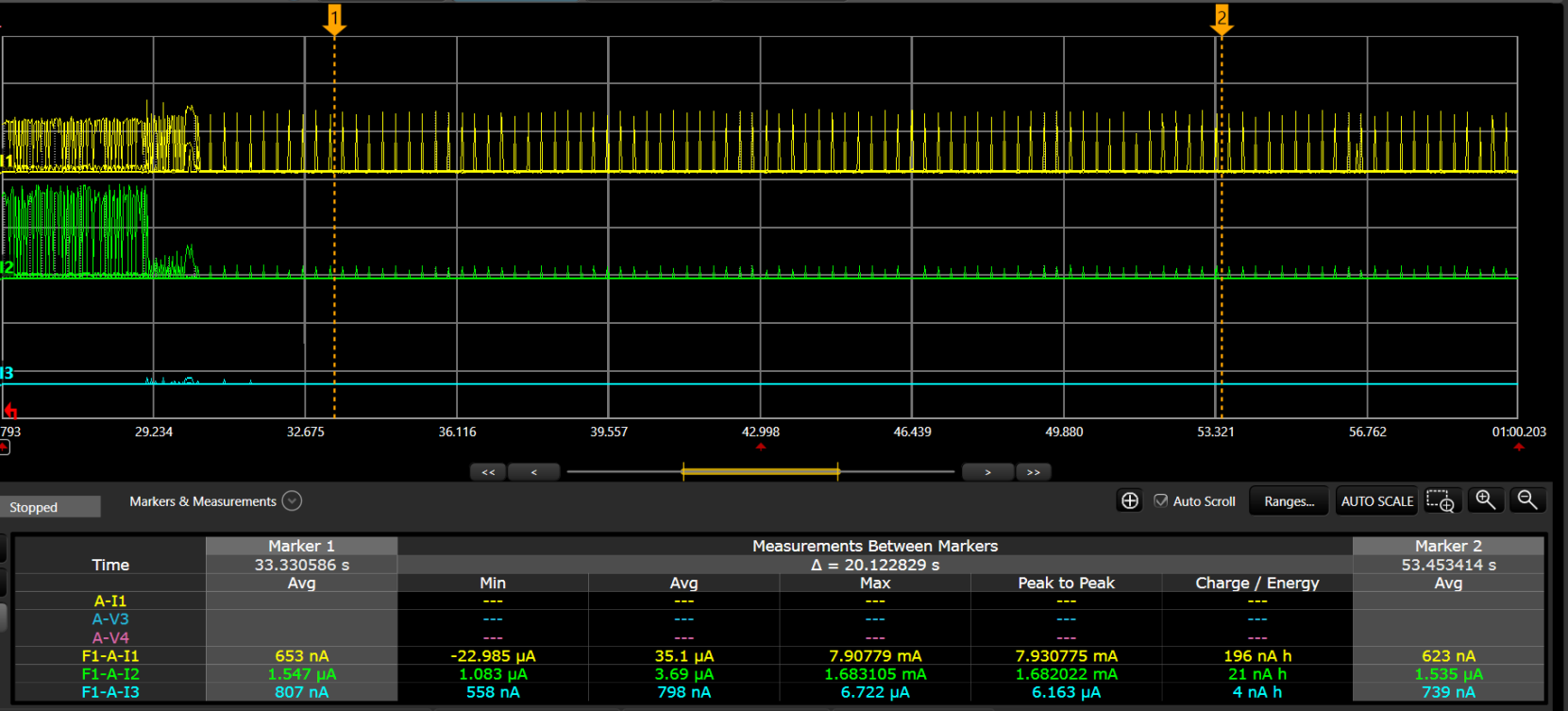
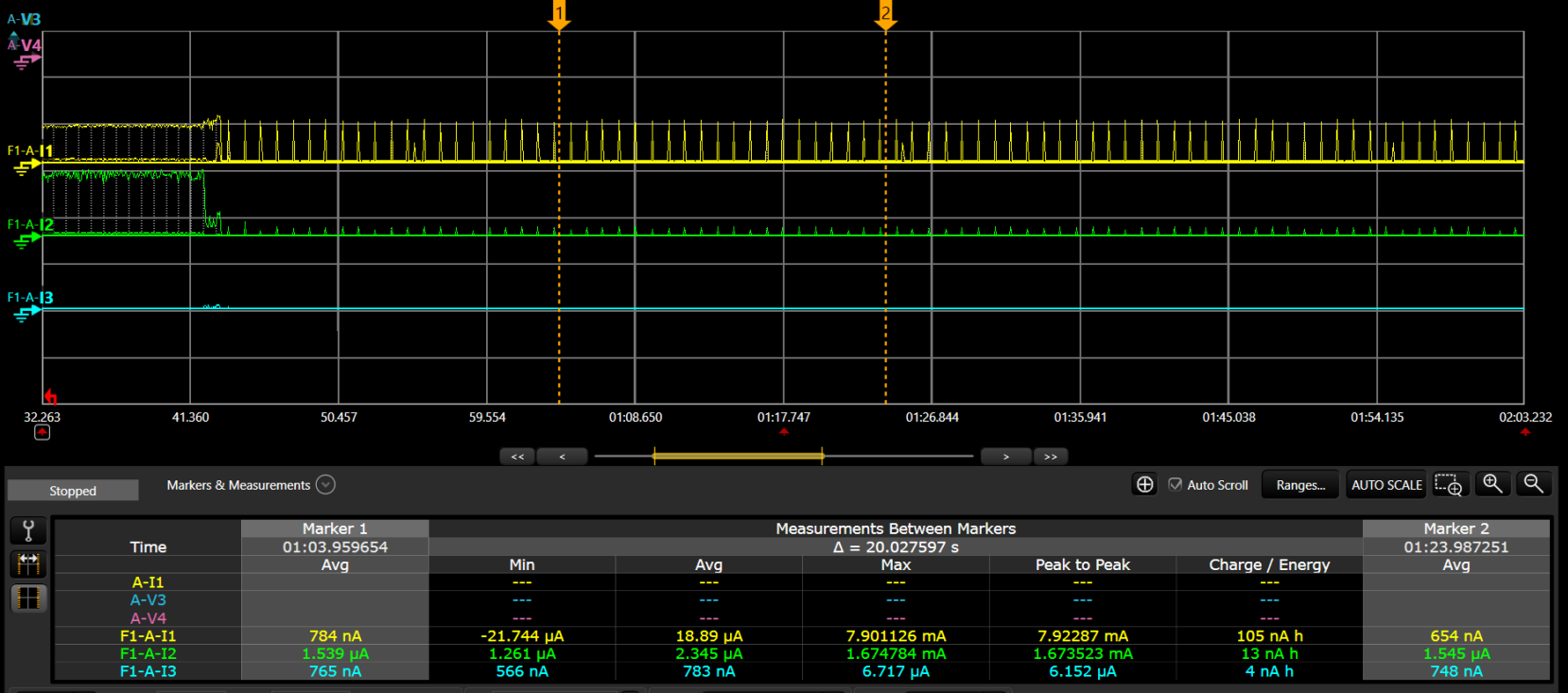
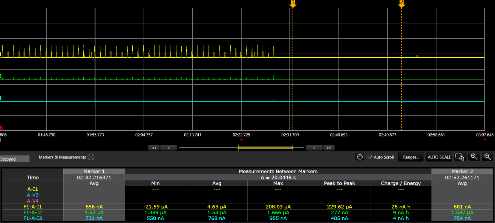
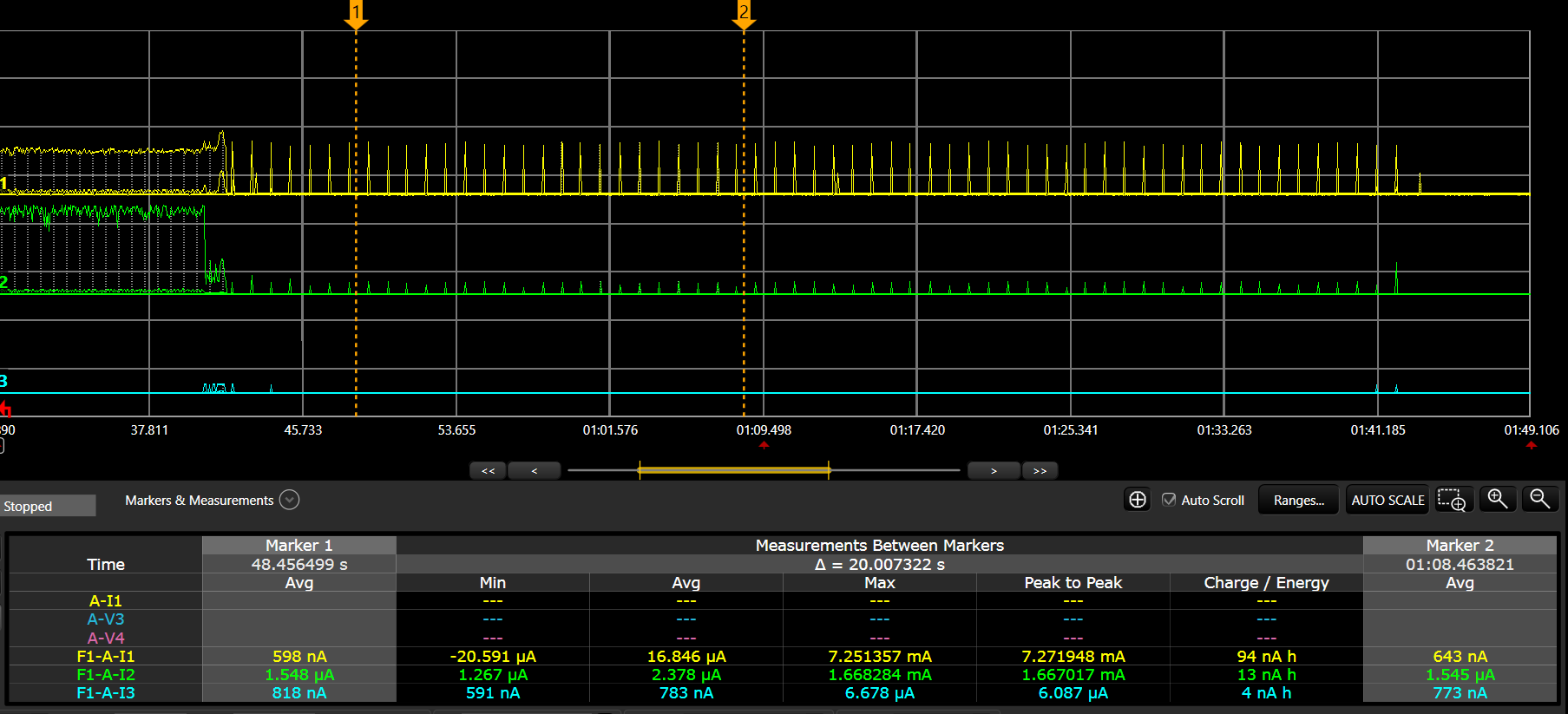
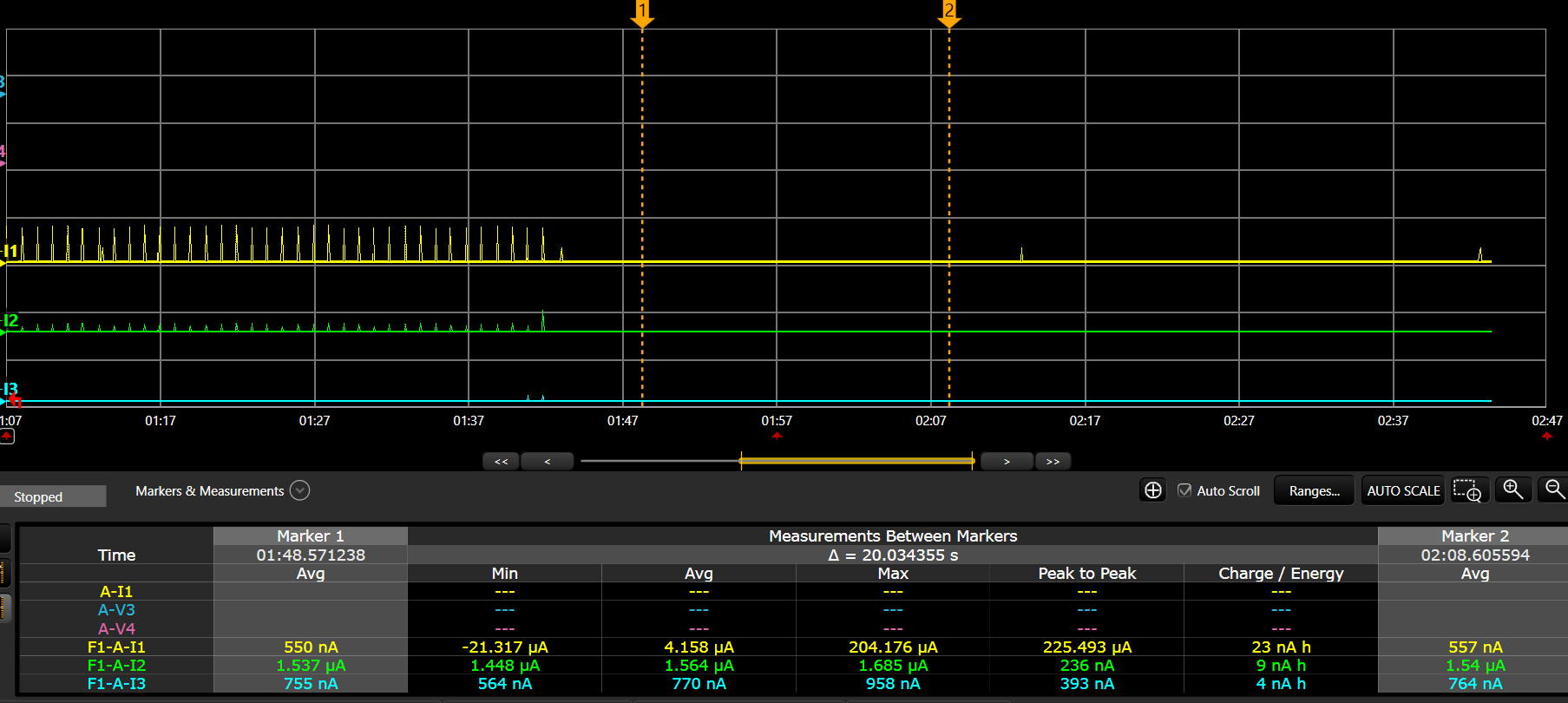
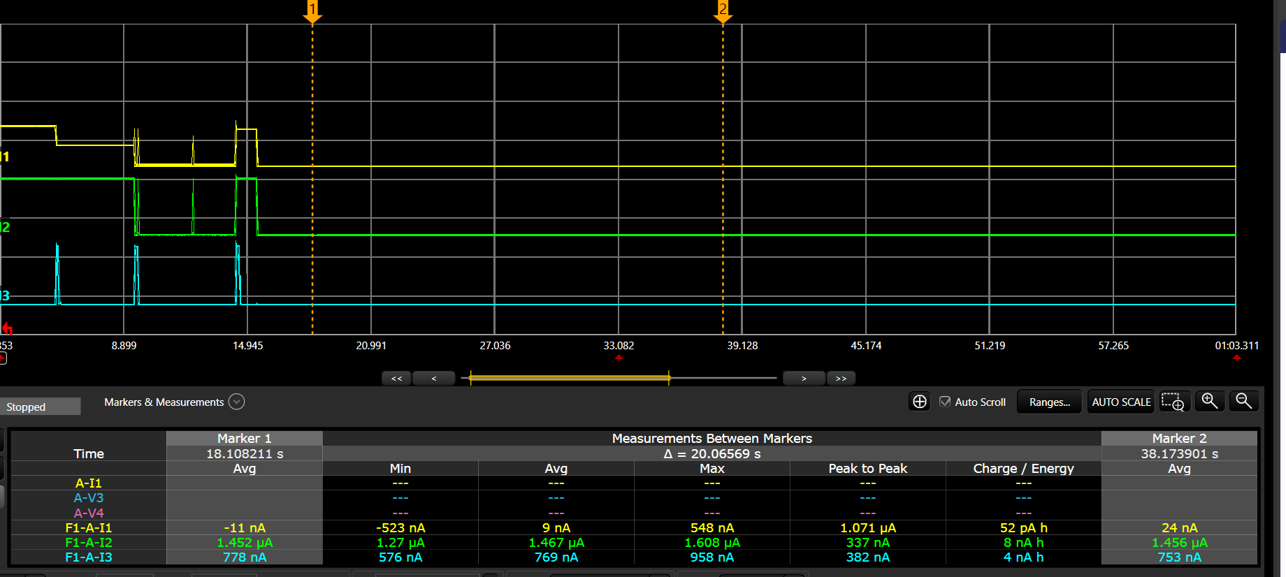
In the following current measurement diagrams, the yellow lines represent the VBAT current, green lines represent VDDPA, and the blue lines represent VDDIO.
Sleep mode
Deep Sleep mode
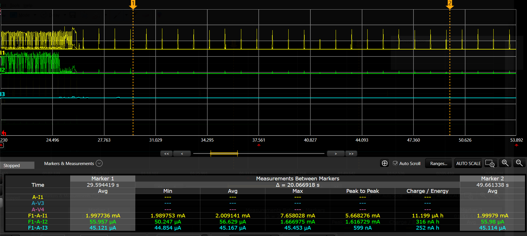
The current consumption is measured when the device is in Deep Sleep; it consumes 4.6 µA at VBAT, 1.5 µA at VDDPA, and 0.76 µA at VDDIO as shown in Figure 22, which is significantly less than Active mode.
When it comes to connection idle state during Deep Sleep, the current consumption is at 35 µA for VBAT at 300 ms connection interval as shown in Figure 20. Current consumption during connection idle can be reduced further by increasing the connection interval. By increasing the connection interval in Deep Sleep from 300 ms to 1 s, the average current consumption is drastically reduced to 18.8 µA as shown in Figure 21.
Deep Sleep RAM mode
The current consumption is measured when the device is in Deep Sleep RAM mode; it consumes 4.1 µA at VBAT, 1.5 µA at VDDPA, and 0.77 µA at VDDIO as shown in Figure 24, which is significantly lower than Active mode.
Hibernate mode
Measured current readings for various power modes
| Connection idle with 1 s connection interval | ||||
|---|---|---|---|---|
| Power rails | Sleep | Deep Sleep | Deep Sleep RAM | Hibernate |
|
VBAT |
2 mA |
18.89 µA |
16. 8µA |
NA |
|
VDDPA |
56 µA |
2.3 µA |
2.3 µA |
NA |
|
VDDIO |
45 µA |
0.78 µA |
0.78 µA |
NA |
| Disconnection idle | ||||
|---|---|---|---|---|
| Power rails | Sleep | Deep Sleep | Deep Sleep RAM | Hibernate |
|
VBAT |
1.9 mA |
4.6 µA |
4.1 µA |
9 nA |
|
VDDPA |
55 µA |
1.5 µA |
1.5 µA |
1.4 µA |
|
VDDIO |
44 µA |
0.76 µA |
0.77 µA |
0.76 µA |
| Connection idle with 1 s connection interval | ||||
|---|---|---|---|---|
| Power rails | Sleep | Deep Sleep | Deep Sleep RAM | Hibernate |
|
VBAT |
2 mA |
20 µA |
18.5 µA |
NA |
|
VDDPA |
56 µA |
2 µA |
2.1 µA |
NA |
|
VDDIO |
45 µA |
0.78 µA |
0.78 µA |
NA |
| Disconnection idle | ||||
|---|---|---|---|---|
| Power rails | Sleep | Deep Sleep | Deep Sleep RAM | Hibernate |
|
VBAT |
1.9 mA |
5.8 µA |
5.3 µA |
1.19 µA |
|
VDDPA |
55 µA |
1.2 µA |
1.3 µA |
1.2 µA |
|
VDDIO |
44 µA |
0.76 µA |
0.76 µA |
0.76 µA |
References
-
Code examples
Code examples for ModusToolbox™ software – Visit this page for a comprehensive collection of code examples
-
Device documentation
-
Development kits
-
Tool documentation
Eclipse IDE for ModusToolbox™ - The Infineon IDE for IoT designers
-
Arm® documentation
Revision history
| Document revision | Date | Description of changes |
|---|---|---|
|
** |
2024-02-27 |
Initial release |
| *A | 2024-04-19 | Updated template; no content update |
Trademarks
The Bluetooth® word mark and logos are registered trademarks owned by Bluetooth SIG, Inc., and any use of such marks by Infineon is under license.