About this document
Scope and purpose
This application note explains the detailed test setup for long range transmission using the AIROC™ CYW20829 Bluetooth® LE SoC. The firmware used in this application is provided as a code example with the ModusToolbox™ software development kit.
Intended audience
This application note is intended for those who wants to integrate the Bluetooth® LE long range feature on CYW20829.
Introduction
The AIROC™ CYW20829 has best-in-class RF link budget with an integrated power amplifier providing 10 dBm of transmit output power and receive sensitivity of -98 dBm for LE 1 Mbps and -106 dBm for LE long range 125 Kbps. The long range claims up to 2.3 KM.
AIROC™ CYW20829 Bluetooth® LE SoC
CYW20829 is a dual-core Arm® M33 device where one M33 core reserved as a Bluetooth® controller, and the other M33 core for customer applications. The CPU subsystem provides 256-KB RAM, XIP interface for external flash, and a rich set of peripherals to enable a diverse set of applications.
The AIROC™ CYW20829 is supported by the ModusToolbox™ development environment, which enables developers to accelerate time-to-market for Bluetooth®-enabled IoT solutions.
Long range application
Figure 1 illustrates the block diagram of the long-range application using the CYW20829 Bluetooth® LE SoC. The application includes a combination of peripheral and central devices. The LE long-range peripheral configures the device as Bluetooth® LE GATT Server, and the LE long-range central application configures the device as Bluetooth® LE GATT Client.
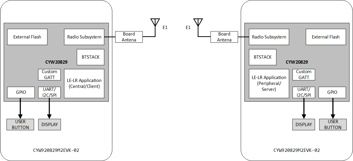
The peripheral device implements a custom GATT Server profile that includes the following services:
- Hello Sensor custom service
- Device Information service
- Battery level service
The Hello Sensor service includes a custom Notify characteristic, which sends a notification or indication to the peer client device upon connection.
The application uses a UART to send debug messages on a UART terminal emulator. The peripheral device starts to advertise its presence using LE-LR PHY when a button press is detected. Similarly, central device scans for the peripheral device upon button press. After an LE connection is established, the central device registers for notifications by using the CCCD handle of the Notify characteristic. Because the CCCD handle of the Notify characteristic requires write authentication, an attempt to enable notification/indication triggers the pairing process at the central side. After the pairing process completes, the peer device's link keys and addresses are stored in the device's flash memory and, therefore, bonded. The user button on the peripheral board is configured to trigger an interrupt on the falling edge. When this button is pressed, the device switches the coding algorithm between S=2 and S=8 and notify using the modified coding algorithm.
Bluetooth® spec for PHY
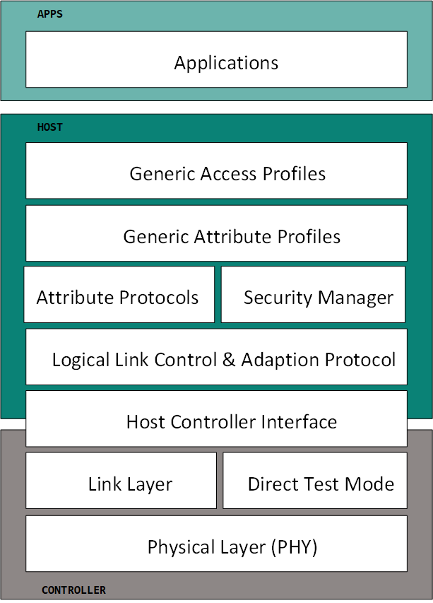
The Bluetooth® technology is a full protocol stack. The bottom layer of this stack is called the Physical Layer and is normally referred to as PHY.
Bluetooth® 5 adds two new PHY variants to the PHY specification, compared to the previous version. Each PHY variant has its own particular characteristics and is designed with specific objectives. The three PHYs, LE 1M, LE 2M, and LE Coded, are referenced in specifications.
LE 1M is the PHY used in Bluetooth® 4 and earlier versions. It uses Gaussian Frequency Shift Keying (GFSK) and has a symbol rate of 1 Msps. Higher up the stack, this correlates to a bit rate of 1 Mbps since one symbol corresponds to one data bit. LE 1M continues to be available for use in Bluetooth® 5 and in fact, its support is mandatory.
The new LE 2M PHY allows the physical layer to operate at 2 Msps and so enables higher data rates than LE 1M. Its support in a Bluetooth® chip is optional.
The LE Coded PHY allows the range to be quadrupled (approximately), compared with Bluetooth® 4, and this is achieved without increasing the required transmission power.
LE Coded PHY implementation
The LE Coded PHY can be used with two different coding schemes: S = 2 and S = 8. The Pattern Mapper converts each bit from the convolutional FEC encoder into P symbols, where the value of P depends on the coding scheme used. If S = 2, there is no change (i.e. P = 1). If S = 8, each bit from the FEC encoder produces 4 output bits (i.e. P = 4) from the Pattern Mapper. The specifics are described in this section.
The choice of the coding scheme, S = 2 or S = 8, with the LE Coded PHY has two consequences. When two symbols represent 1 bit, the PHY data rate is 500 Kbps; for S = 8 (where 8 represents 1 bit), the PHY data rate is 125 Kbps.
Due to the requirement for redundant data to support the FEC algorithm at the receiver end, it also impacts the number of symbols, which must be transmitted and hence reduces the overall data rate. Specifically, one bit which passed through both the FEC Encoder and the Pattern Mapper becomes 2 bits when S = 2 or 8 bits when S = 8. The following table explains this.
| Input | Output with S = 2 | Output with S = 8 | Data rate |
|---|---|---|---|
| 0 | 0 | 0011 | 125 kb/s or 500 kb/s |
| 1 | 1 | 1100 | 125 kb/s or 500 kb/s |
LE Coded PHY packet format
The packet format defined for the LE Coded PHY is shown in Figure 3.
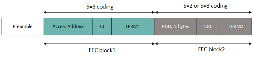
Each packet consists of the Preamble, FEC block 1, and FEC block 2.
- The Preamble is not coded
- The FEC block 1 consists of three fields: Access Address, Coding Indicator (CI), and TERM1. CI determines which coding scheme is used for FEC block 2
- The FEC block 2 consists of three fields: PDU, CRC, and TERM2. These shall use either the S=2 or S=8 coding scheme depending on the value of the CI
The entire packet is transmitted with 1 Msym/s modulation.
Hardware setup
CYW20829 evaluation board
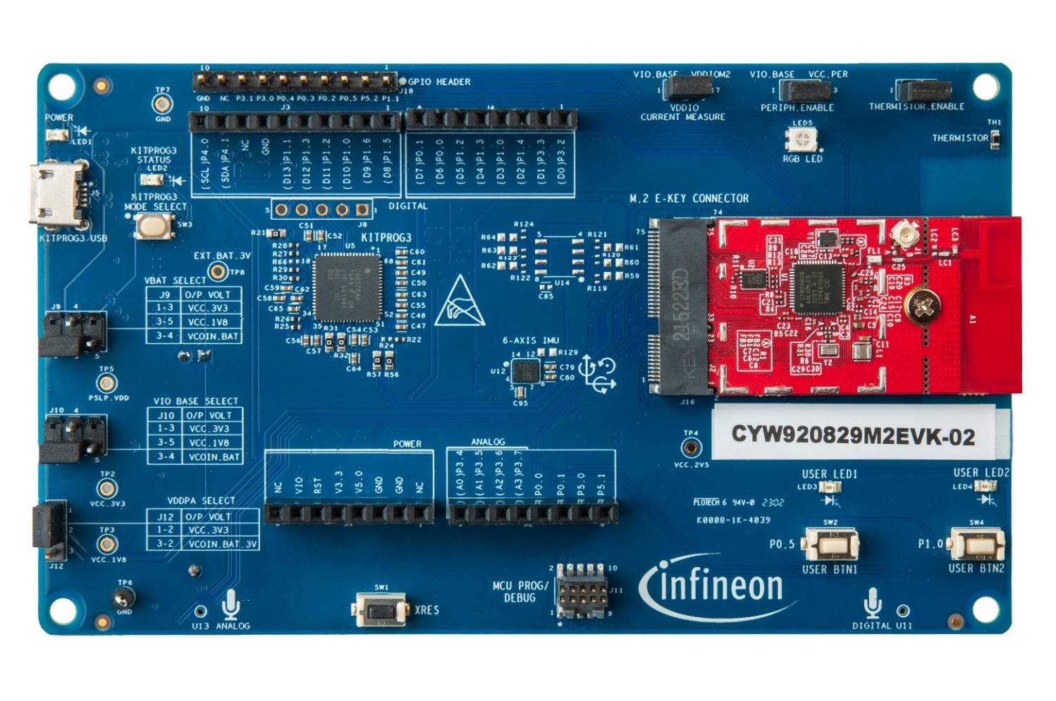
The CYW20829 M.2 board (CYW920829M2IPA2) consists of the 56-pin silicon target device on a custom pinout M.2 card that is interfaced with the base board (CYW9BTM2BASE3-01). The CYW20829 silicon pins should be brought out to the base board through the M.2 connector, featuring the peripherals such as UART, I2C, to be used with sensors and displays. The board is powered using a USB micro type B cable. Refer to the CYW920829M2EVK-02 kit user guide for more information.
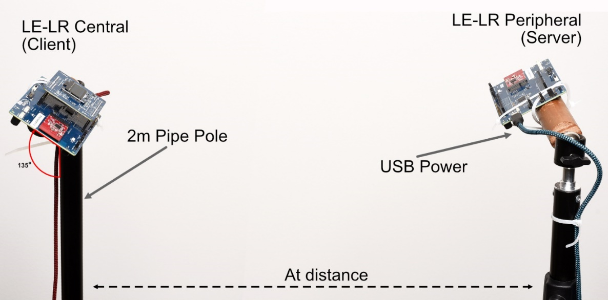
LE-LR test setup
Two evaluation boards are used to set up the LE-LR demo. The CYW920829M2EVK-02 board is used with CYW920829M2IPA1 (M.2 Card), which uses the PCB-based antenna.
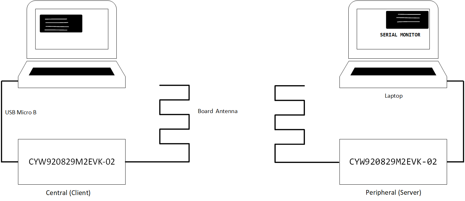
Figure 5 shows the setup block. Both the evaluation kits are connected to the laptop over a 2-meter long USB cable. The boards are mounted on the 2-meter long pipe. The boards are powered using the same USB connector and the serial logs are captured in the laptop with a serial monitor. One board is configured as a server (peripheral) and the other is configured as a client (central). The optional display shield is used on the client side to show the connection details and RSSI values on the OLED screen. The user buttons on the EVK are used to initiate the connection between the two boards. Refer to Section 5 for the test sequence. Figure 6 shows the actual setup.
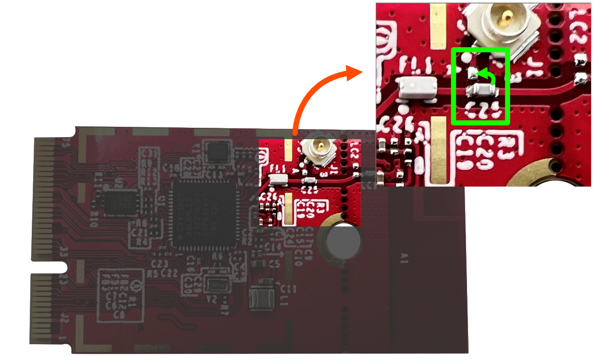
External antenna
The external antenna is one of the preferred options to use in the long-range application. To use the external antenna, switch the capacitor (C25) on the CYW920829M2IPA1 (M.2 Card) towards the external antenna path, as shown in Figure 7.
User buttons
The user button (SW2) on the EVK is used for the following:
- Initiate the advertisement on the server side and initiate the scanning on client side
- Switch the coding scheme between S=2 and S=8 after the connection is established
Reset button (SW1) is used to re initiate the application on central & peripheral side.
Display shield
The display shield is optional and can be used to show the coding scheme, RSSI values, and connection status etc. The user can enable or disable the display shield in the firmware setting (makefile).
Software and tools
This section explains the required software tools to create and build the long-range application for testing.
ModusToolbox™
ModusToolbox™ software is a modern, extensible development environment supporting a wide range of Infineon microcontroller devices. It provides a flexible set of tools and a diverse, high-quality collection of application-focused software. These include configuration tools, low-level drivers, libraries, and operating system support, most of which are compatible with Linux-, macOS-, and Windows-hosted environments.
Refer to the Eclipse IDE for ModusToolbox™ user guide for more details.
Code examples
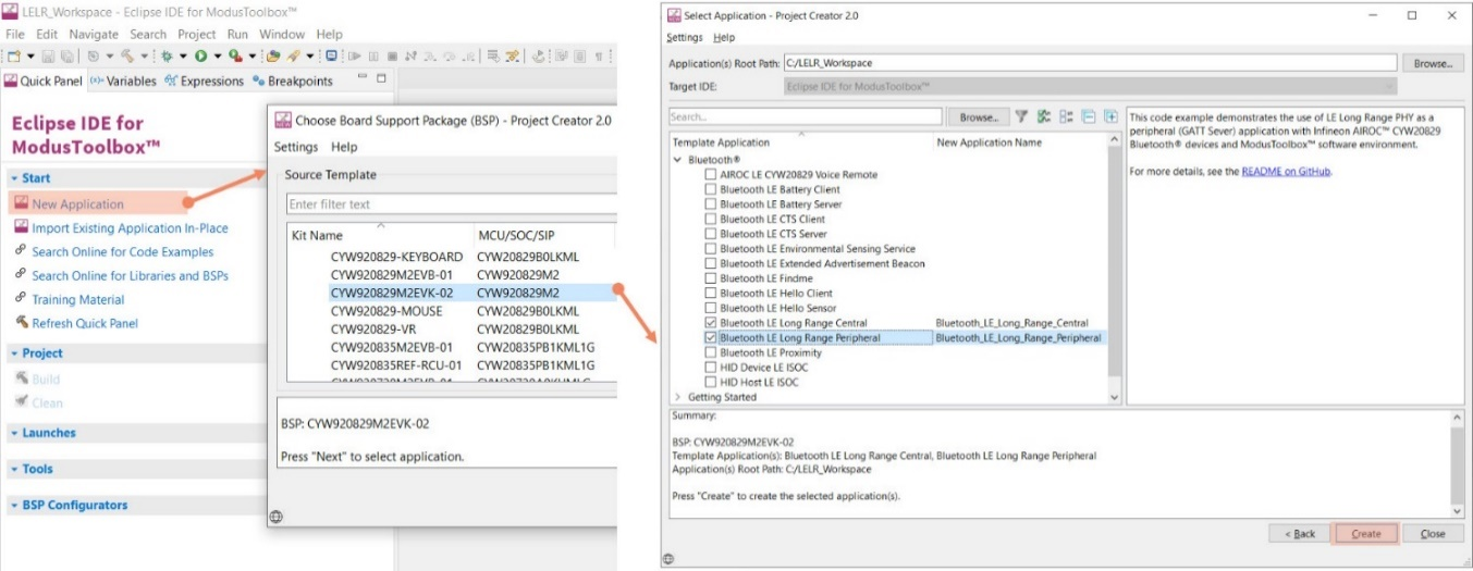
ModusToolbox™ code examples can be found through the GitHub code example page. The following two example codes are required to run the LE-LR application:
Import these examples using the Project Creator tool, as shown in Figure 8, to create an application and use it directly with ModusToolbox™ tools.
LE LR central application
This is a GATT client application designed to connect and access the services of the server device (Hello Sensor) using the LE-LR PHY. This application has the following features:
- LE Stack registration for various events
- Connecting to the peripheral
- Processing the notification from the server
- Scan and connect to the peer over the LE Coded PHY
- Switch between S = 2/S = 8 PHY coding algorithms
For more details, refer to the central application’s README.md.
LE LR peripheral application
This is a GATT server application designed to obtain the sensor data (simulated) and connect to the client application using the LE-LR PHY.
- LE Stack registration for various events
- Connecting to the client
- Sending the notification data
- Connect over LE Coded PHY
For more details, refer to the peripheral application’s README.md.
Build and flash the firmware
The LE-LR application can be built within ModusToolbox™ or the ModusShell cmd line. The binary is generated in the build folder. The firmware can be loaded into the Eval kits using KitProg3 or using an external SWD with Cypress Programmer. Refer to the Cypress Programmer user guide for more details.
Testing and results
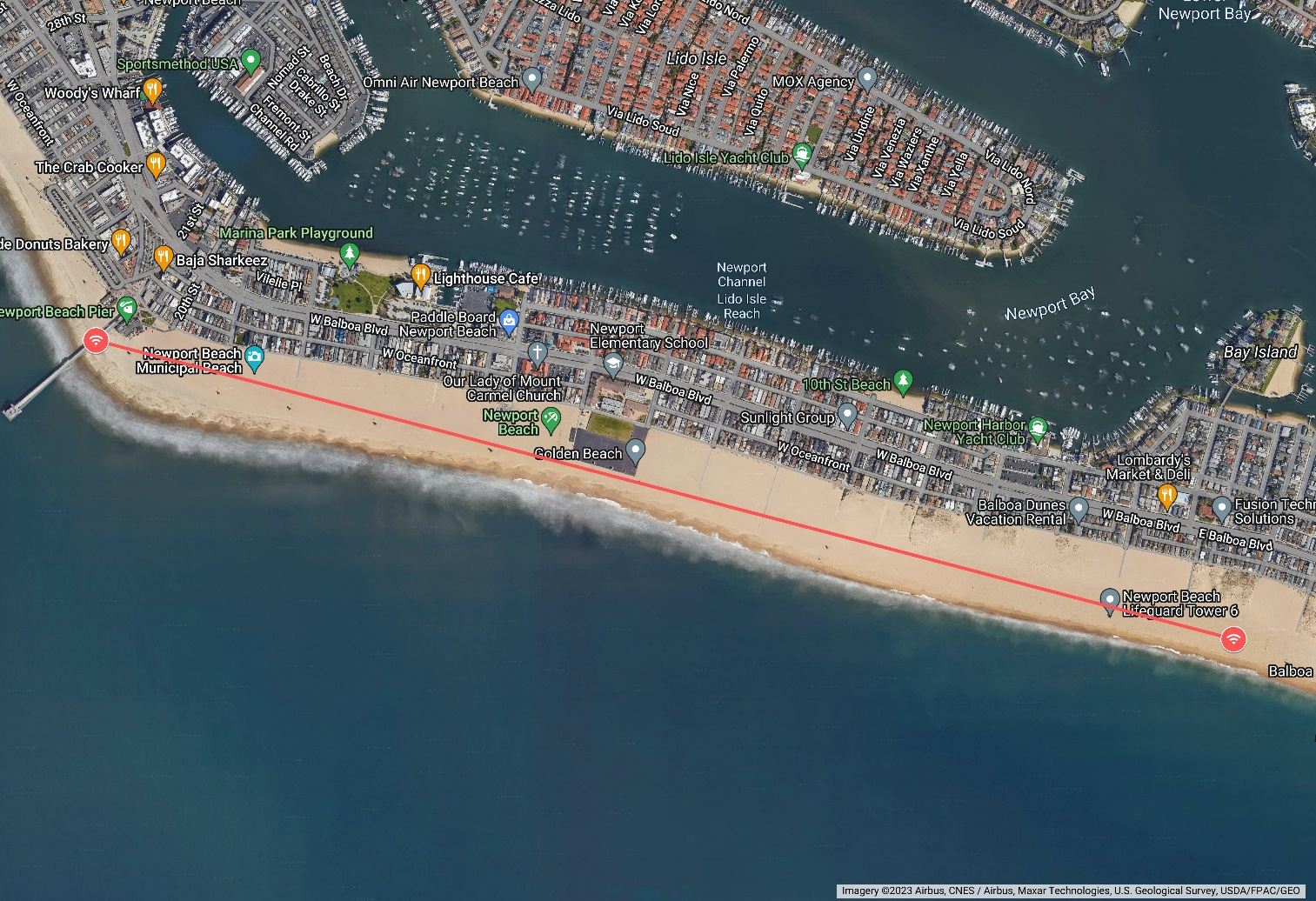
Testing is performed at Newport Beach, CA, to get a clear line of sight, and less environment radio noise.
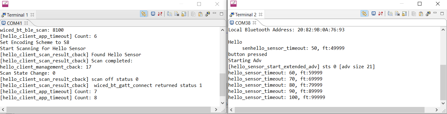
Test procedure
- Connect the board to the laptop and download the firmware
- Press SW1 (Reset) on both the peripheral and central devices to initialize the application
- Wait for some time for the applications to start and print log messages on the console
- Press SW2 on the peripheral device to start the advertisement
- Press SW2 on the client device to start discovering the server and connects to it
- Once the connection is established, the logs start printing RSSI values and time counter values. If the display is used, the details are showed on the display as well
- Take any one board to move far away; the distance is calculated to be around 2.3 KM
- If there is a disconnection in between, the client tries to re-establish the connection with server
Noise interference
Noise and interference are the largest contributors to poor range in a long-range testing environment. In the real world, increased noise means your Bluetooth® devices may disconnect at ranges far shorter than advertised. To improve SNR, it is important to reduce the noise and interference during testing. To reduce interference, make sure to test in the morning and walk away from people to reduce the impact of noise. Maintain a line of sight, or LoS, connection between the peripheral and central devices at all times.
People often carry multiple devices that operate on the 2.4-GHz band, such as their smartphones, smartwatches, and wireless earbuds. Just as a building’s walls may inhibit Bluetooth® range, other physical objects, such as beach umbrellas or lifeguard towers, also contribute to multipath, and may absorb radio frequency energy. Multipath occurs when radio signals propagate between two antennas via multiplate paths. Multipath is undesirable, as it can lead to interference and distortion of a wanted signal. In the real world, LoS between devices may not be plausible. We actively monitored the Received Signal Strength Indicator (RSSI), of the receiver and adjusted the walking path along the beach during testing to keep the RSSI higher than the maximum S8 Coded PHY sensitivity. The maximum output power of the CYW20829 MCU is 10 dBm using the internal power amplifier, and the Coded PHY helps to improve the maximum sensitivity of to -106 dBm. The Link budget is the sum of the absolute value of all gains and losses of a radio frequency system in decibels. In an ideal environment, the maximum link budget is |10 dBm| output power + |-106 dBm| sensitivity = 116 dB.
Antenna orientation
Antenna directivity is a measure of the amount of radiated energy moving in a particular direction, while antenna gain takes both an antenna’s directivity and efficiency. Antennas do not radiate with the same power in all directions, as shown in Figure 11. To determine the directions in which the kit radiates the strongest, the antenna gain of the CYW920829M2EVK-02 kit is measured.. Different Bluetooth® antenna radiate most optimally in different directions, which influence the directions in which the boards face during testing. Since the directivity of an antenna when transmitting is identical to the directivity of an antenna when receiving, both the boards were placed facing each other, taking into consideration the maximum antenna gain (see Figure 6). The CYW920829M2EVK-02 kit is considered a “directional” antenna, as the radiation pattern is strongest in one particular angular direction.
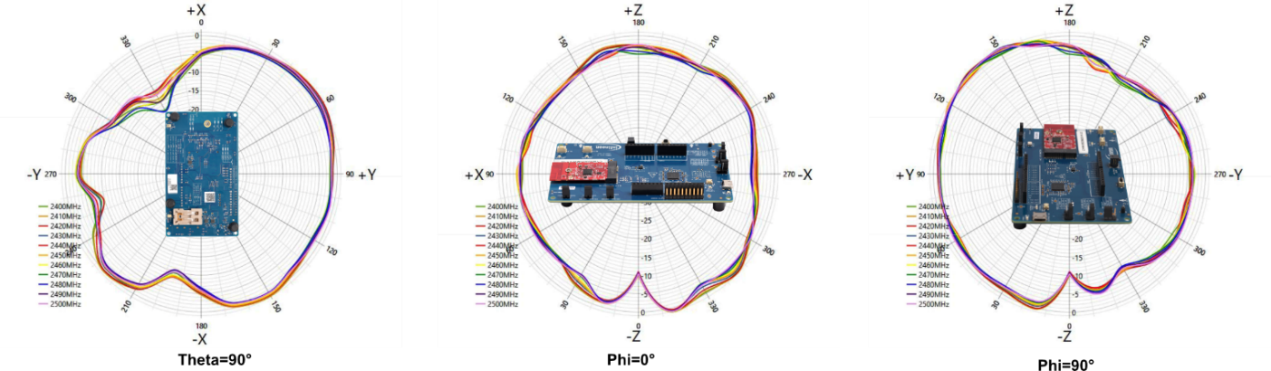
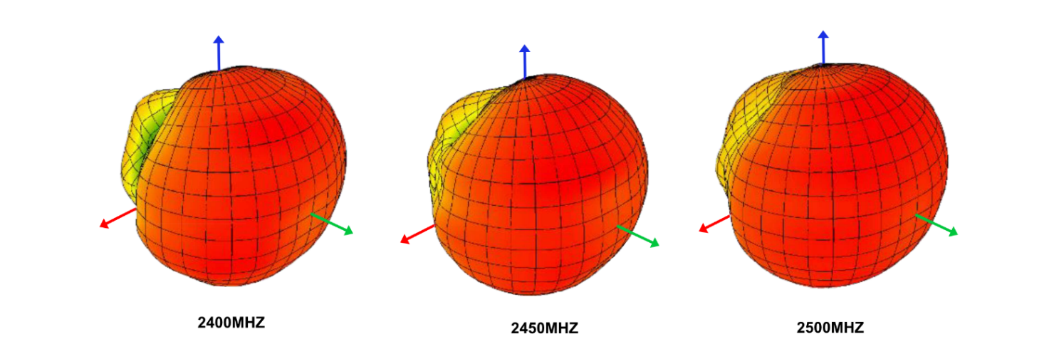
Antenna radiation
The antenna radiation is tested across different frequencies. Figure 12 shows the radiation pattern for difference frequencies with maximum antenna gain orientation.
Power estimation
The power consumption for the LE-LR application is calculated during the connected state between the central and peripheral devices. Figure 13 shows the current measurements for 1-minute duration.
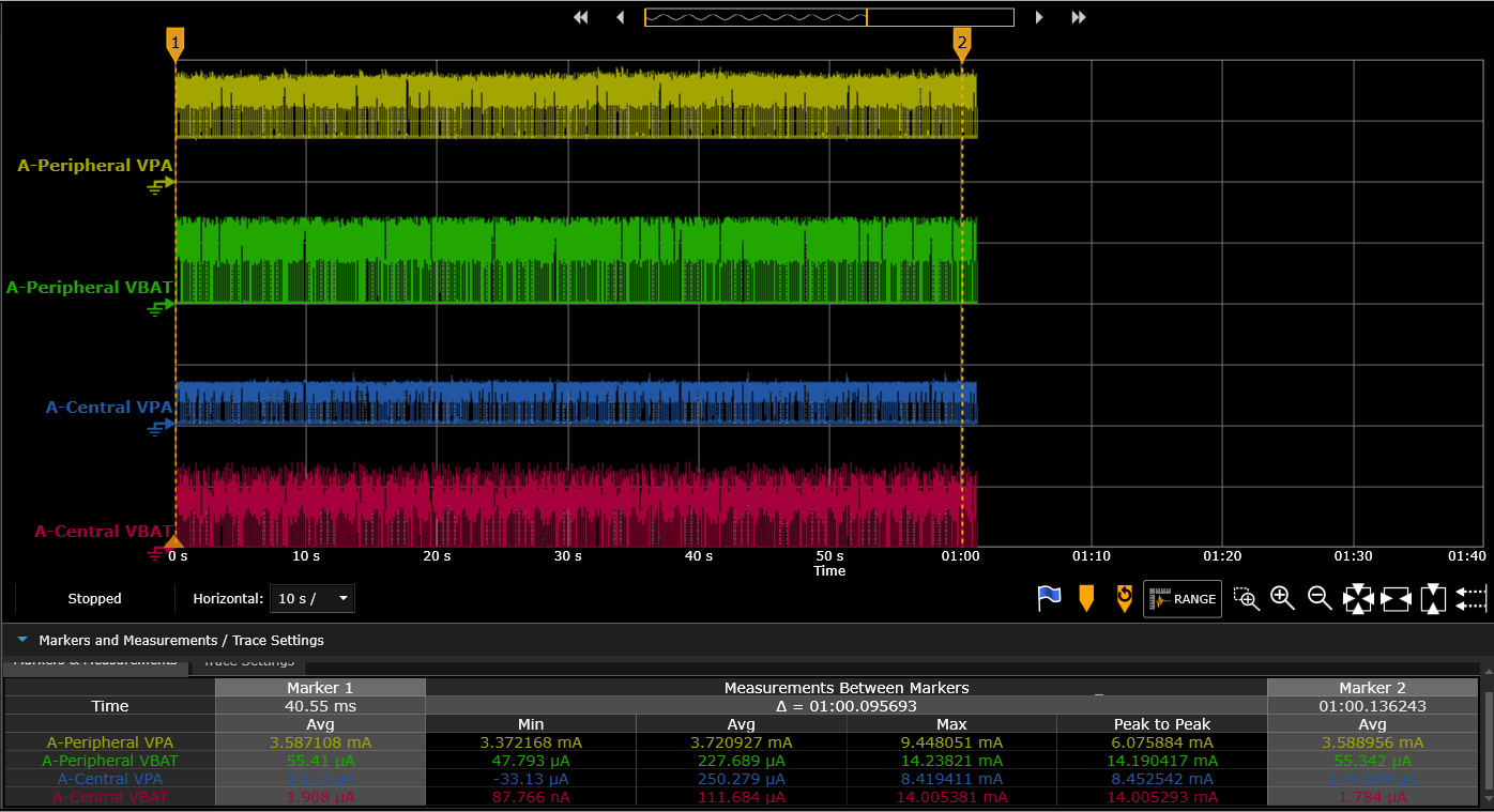
The current measurement is performed at different ranges and the values are shown in the following table:
| Device mode | VPA Avg. current | VBAT Avg. current | VDDIO Avg. current | Total current | RSSI |
|---|---|---|---|---|---|
| Peripheral | 3.72 mA | 227.68 µA | 41.446 µA | 3.989 mA | -55 dBm |
| Central | 250.27 µA | 111.68 µA | 2.671 µA | 362 µA | -55 dBm |
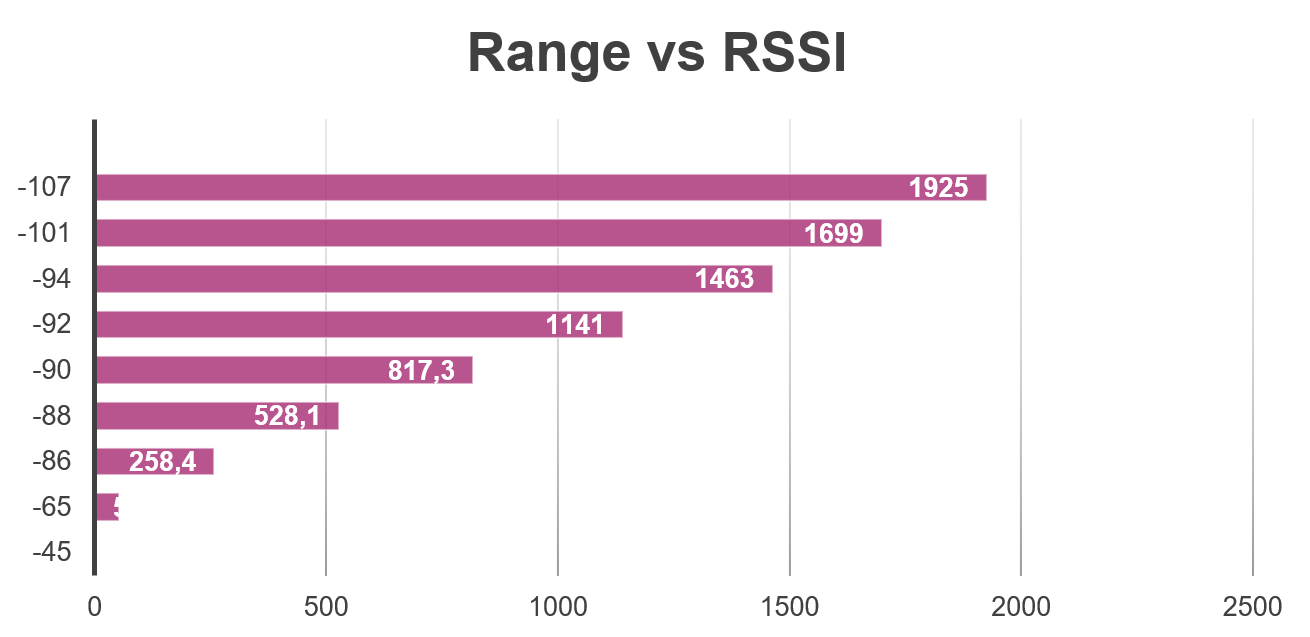
Range vs RSSI value
The RSSI values are captured at every second along with transmission data. The distance versus the RSSI values are plotted in Figure 14 (the distance values in the horizontal axis are in meters).
Bluetooth® range estimator
The Bluetooth® range estimator tool from Bluetooth® SIG used to estimate the range of Bluetooth® with parameters.
References
Revision history
| Document revision | Date | Description of changes |
|---|---|---|
| ** | 2023-09-12 | Initial version |
| *A | 2024-06-11 | Template update; no content update |
Trademarks
The Bluetooth® word mark and logos are registered trademarks owned by Bluetooth SIG, Inc., and any use of such marks by Infineon is under license.