About this document
Scope and purpose
This document provides hardware guidance on how to design a two-layer PCB with CYW20829.
Intended audience
This document is intended for hardware engineers creating two-layer PCB layout designs with CYW20829.
Introduction
This document provides basic guidelines on the two-layer PCB layout for CYW20829.
Document structure
- Section 2, Schematic design considerations provides the schematic design considerations.
- Section 3, Component placement for two-layer PCB explains the component placements and recommended parts for the critical components.
- Section 4, PCB layers and routing provides the routing guidelines and the recommended trace width for various power traces.
Schematic design considerations
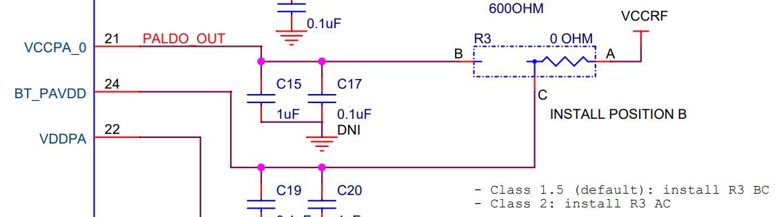
PAVDD supply for CYW20829
- For CYW20829 Class 1.5, BT_PAVDD must be connected to VCCPA_0 (PALDO_OUT (2.5 V))
- For CYW20829 Class 2.0, BT_PAVDD must be connected to VCCRF (RFLDO_OUT (1.2 V))
Crystal specifications and requirements
For the crystal parts, it is recommended to use the following:
- TXC 7R24070007 - 24 MHz main crystal
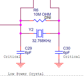
- TAI-SAW TZ3406A - 32.768 kHz crystal
The 24 MHz crystal oscillator must have an accuracy of ±20 ppm as defined by the Bluetooth® specification. Two external load capacitors are required to work with the crystal oscillator. The selection of the load capacitors is dependent on crystal and layout (see Figure 2). The value of the load capacitors needs to be adjusted to be within the ±10 kHz of initial carrier frequency tolerance.
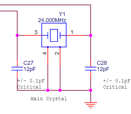
Crystal specifications and requirements for the 24 MHz crystal are shown in Table 1.
| Parameter | Conditions | Minimum | Typical | Maximum | Unit |
|---|---|---|---|---|---|
|
Nominal frequency |
- |
- |
24.000 |
- |
MHz |
|
Oscillation mode |
- |
Fundamental |
- |
||
|
Frequency accuracy |
Includes operating temperature range and aging |
- |
- |
±20 |
ppm |
|
Equipment series resistance |
- |
- |
- |
60 |
W |
|
Load capacitance |
- |
- |
8 |
- |
pF |
|
Drive level |
- |
- |
- |
200 |
µW |
|
Shunt capacitance |
- |
- |
- |
2 |
pF |
The 32 kHz or 32.768 kHz crystal oscillator (optional) must have an accuracy of ±250 ppm or more as per the Bluetooth®specification over temperature and including aging.
The default component values are: C1 = C2 = ~6 pF. The values of C1 and C2 are used to fine-tune the oscillator. Figure 3 shows the 32 kHz XTAL oscillator with external components and Table 2 lists the oscillator’s characteristics.
| Parameter | Symbol | Conditions | Minimum | Typical | Maximum | Unit |
|---|---|---|---|---|---|---|
|
Output frequency |
Foscout |
– |
– |
32 |
– |
KHz |
|
Frequency tolerance |
– |
Over temperature and aging |
– |
– |
250 |
ppm |
|
XTAL drive level |
Pdrv |
For crystal selection |
– |
– |
0.5 |
µW |
|
XTAL series resistance |
Rseries |
For crystal selection |
– |
– |
70 |
kΩ |
|
XTAL shunt capacitance |
Cshunt |
For crystal selection |
8 |
– |
2.2 |
pF |
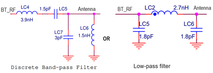
RF filter
A bandpass or low-pass filter is needed to depress the harmonic frequency, which is placed between the antenna matching components and the CYW20829 device. A four-element discrete filter requires Hi-Q components. The component values may vary depending on the layout and required optimization.
Figure 4 shows the reference circuit.
Programming interface
CYW20829 adopts MiniProg4 as a programming and debug kit. A 5-pin or 10-pin connector is needed to connect to MiniProg4 (see Figure 5).
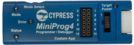
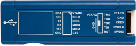
The 5-pin connector is configured in a single row with a 100-mil pitch. The suggested mating connector part number is Molex Connector Corporation 22-23-2051.
The 10-pin connector is configured as a dual row with 50-mil pitch. It is used with a ribbon cable (provided) to mate to a similar connector on the target board. The suggested mating connector part number is CNC Tech 3220-10-0300-00 or Samtec Inc. FTSH-105-01-F-DV-K-TR.
If there is not enough space to place a connector, use test points for jump wire.
HCI UART interface
To run a Bluetooth® LE PHY test with Bluetooth® test equipment such as R&S CMW270, the HCI UART interface is needed. The following GPIOs are defined as HCI UART interface.
| GPIO | Description |
|---|---|
|
P3.1 |
HCI UART RTS |
|
P3.2 |
HCI UART RX |
|
P3.3 |
HCI UART TX |
|
P4.0 |
HCI UART CTS |
To connect these GPIOs, a connector or test points are necessary. These GPIOs can be used for other functionality as well.
Component placement for two-layer PCB
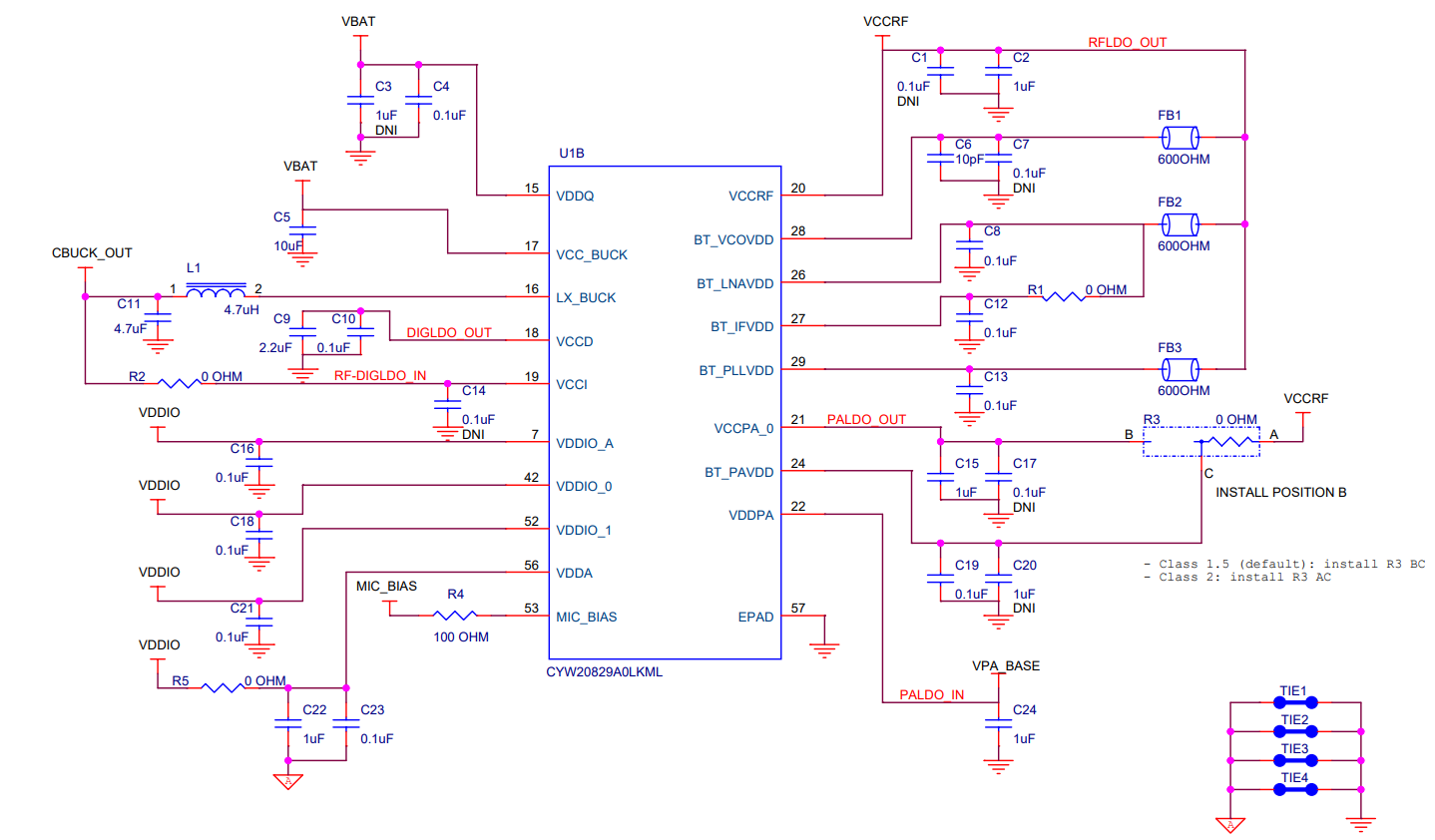
A two-layer PCB is possible for CYW20829 design to optimize cost. As a rule, the order of the front-end component placement should follow the received signal flow from the antenna to the antenna matching circuit, filter circuit, and to the chip RF pin. Keep radio front end (RF), power management unit (PMU), and baseband (BB) decoupling capacitors as close as possible to the associated CYW20829 pin pads.
Bypass capacitor placement
Figure 7 shows the PMU and the RF front-end section. When making determinations about the part placements on the PCB, the following requirements must be met:
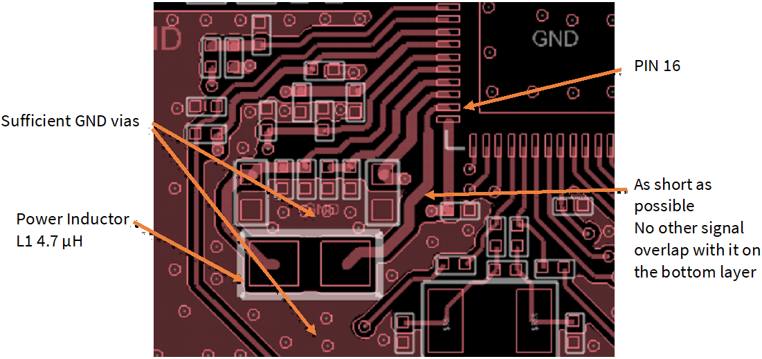
- VBAT inputs, which consist of VDDQ (Pin 15) and VCC_BUCK (Pin 17) must have a 0.1 µF (C4) capacitor placed as close to pin 15 as possible and a 10 µF (C5) capacitor placed as close to pin 17 as possible. The second bypass capacitor on VDDQ (Pin 15) is optional and may be omitted if board space is limited
- Both the 4.7 µH (L1) power inductor and 4.7 µF (C11) capacitor must be placed as close to LX_BUCK (Pin 16) as possible
- The bypass capacitor on VCCI (Pin 19) is optional and may be omitted if board space is limited
- VCCD (Pin 18) must have a 2.2 µF capacitor and a 0.1 µF capacitor placed as close to the pin as possible. Place a 0.1 µF capacitor closer to the pin
- VCCRF (Pin 20) must have a 1 µF capacitor placed as close to the pin as possible. A second bypass capacitor is optional and may be omitted if board space is limited
- BT_VCOVDD (Pin 28) must have a 10 pF capacitor placed as close to the pin as possible. A second bypass capacitor is optional and may be omitted if board space is limited
- BT_LNAVDD (Pin 26) must have a 0.1 µF capacitor placed as close to the pin as possible
- BT_IFVDD (Pin 27) must have a 0.1 µF capacitor placed as close to the pin as possible
- BT_PLLVDD (Pin 29) must have a 0.1 µF capacitor placed as close to the pin as possible
- VCCPA_0 (Pin 21) must have a 1 µF capacitor placed as close to the pin as possible. A second bypass capacitor is optional and may be omitted if board space is limited
- BT_PAVDD (Pin 24) must have a 0.1 µF capacitor placed as close to the pin as possible. A second bypass capacitor is optional and may be omitted if board space is limited
- VDDPA (PIN 22) must have a 1 µF capacitor placed as close to the pin as possible
In the baseband area, the following component placement must also be met:
- VDDIO_A (Pin 7), VDDIO_0 (Pin 42), and VDDIO_1 (Pin 52) must have a 0.1 µF for each pin, and they must be placed as close to the pin as possible
- VDDA (Pin 56) must have a 0.1 µF capacitor and a 1 µF capacitor be placed as close to the pin as possible
Antenna placement
Place the PCB antenna as close as possible to the CYW20829 chip. Always place the antenna in a corner of the PCB with sufficient clearance from the rest of the circuit. Follow the antenna designer’s or manufacturer’s recommended ground pattern for the antenna. Do not place any component, planes, mounting screws, or traces in the antenna keep-out area across all layers. The actual keep-out area depends on the antenna used.
For more details on PCB antennas general guidelines, see AN91445 - Antenna design and RF layout guidelines. For the associated Gerber file, click here.
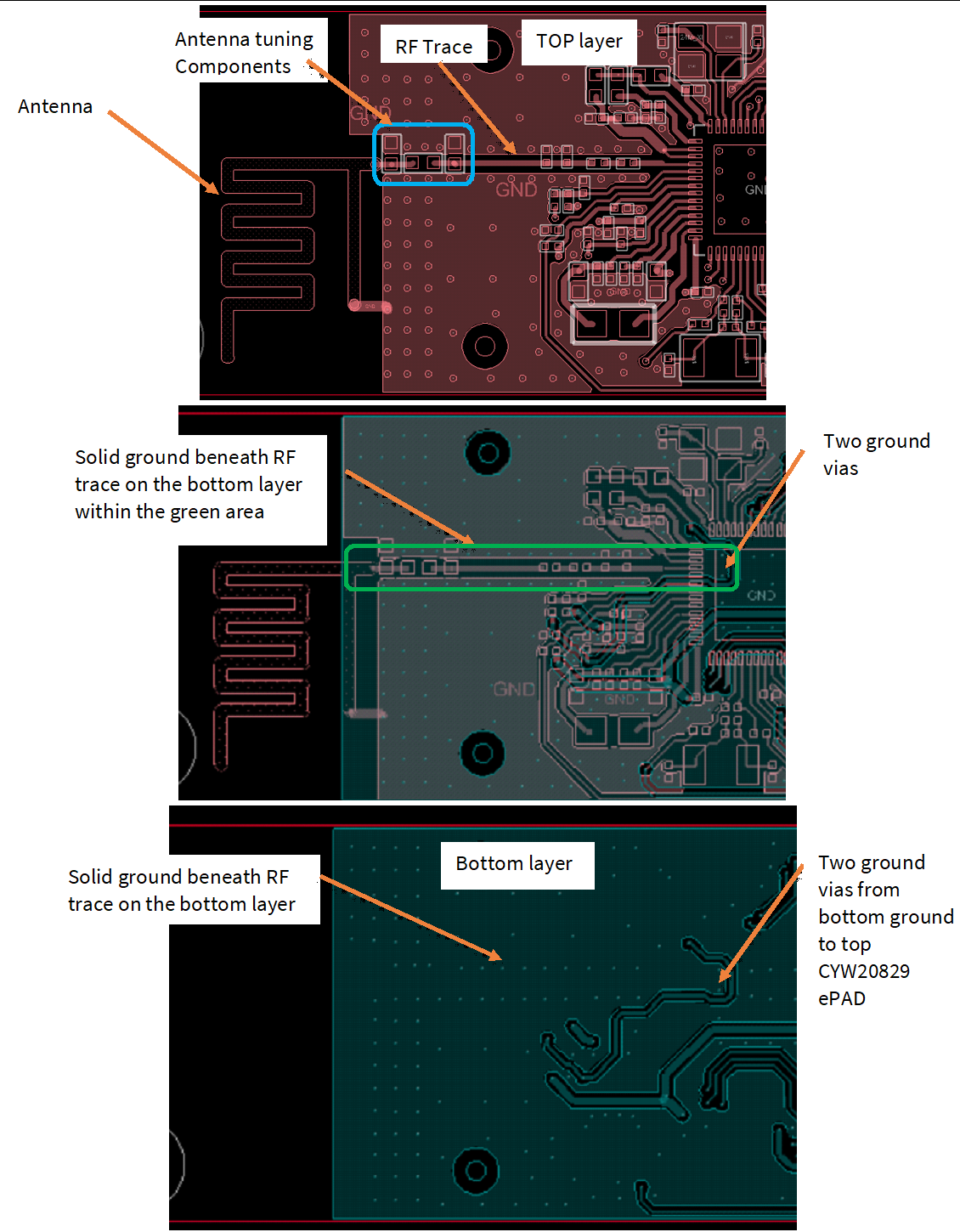
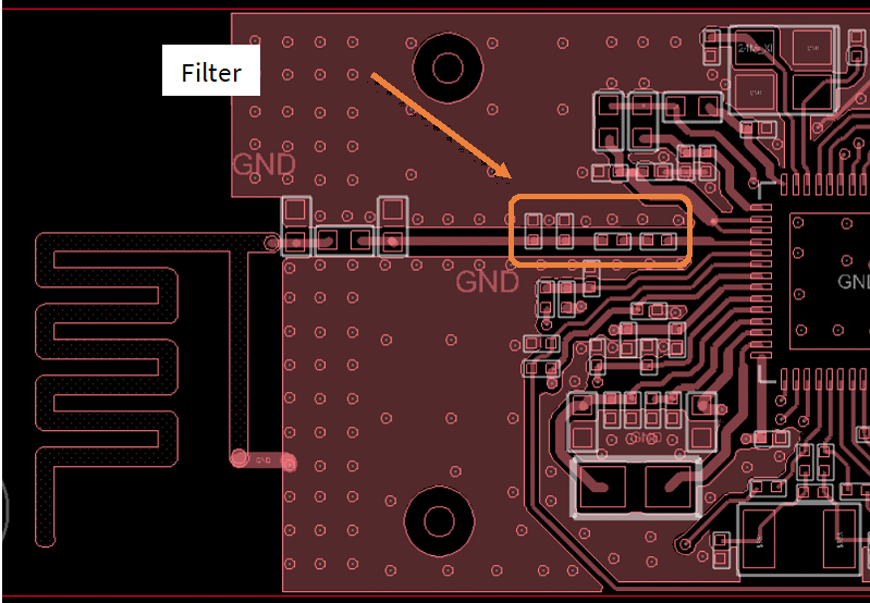
RF filter
Place the filter between the antenna matching components and the CYW20829 device to attenuate harmonics from CYW20829. A 50 Ω impedance microstrip is used for all connections of the filter. Components need to be placed together as closely as possible. Place a GND via as close as possible to the GND pads of the two shunt components.
Insertion loss and out-of-band attenuation performance may vary depending on PCB layouts and component tolerances.
Power inductor placement
The power inductor must have good isolation; this is done by surrounding it with as much ground as possible. The power inductor should also be placed as close to CBUCK_OUT pins (LX_BUCK, Pin 16) as possible. The inductor should be placed adjacent with the output capacitor. The copper on the PCB top layer under this inductor should be cut out. The power inductor part used in the CYW20829 reference design is Murata; DFE201610E-4R7M=P2.
|
Parameter |
Conditions |
Min. |
Typ. |
Max. |
Unit |
|---|---|---|---|---|---|
|
External inductor, L1 |
4.7 μH ±20, 1.6A, DCR = 288 mΩ (for frequency < 1 MHz) |
- |
4.7 |
- |
μH |
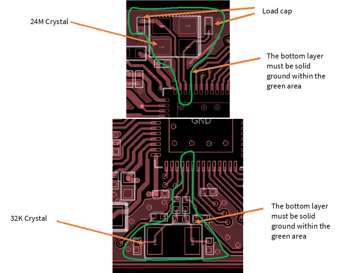
Crystal placement
Protect the crystal and related traces from noise sources and use a solid ground to separate the crystal from RF traces and other signals. The crystal ground plane should have direct vias to the CYW20829 ePAD.
The recommended load capacitor placement is as shown in Figure 11. This placement uses the least amount of PCB trace to connect the CYW20829 chip, the crystals, and the crystal load capacitors, which together will minimize the parasitic capacitance.
PCB layers and routing
Ground vias
Do not use long and thin traces to connect components to ground vias; instead, cover the entire ground pad with ground copper and place the ground vias as close to the ground pad as possible. Via on pad is required for the ground pad of the CYW20829. Only use through hole vias in the open area to stitch the ground plane on all layers together. Ensure that there are enough ground pins near the ground pad of the CBUCK output capacitor (C11 in this design).
TOP Layer: Components, signal fanout, and RF trace
All the passive components of the chip can be placed on the top layer. Signal fanout from the CYW20829 chip will also be done on the top layer.
The RF trace, as shown in Section “Antenna placement” must be well isolated and have a solid ground plane along both sides of the trace. Ensure that this RF trace is 50 Ω impedance matched. Route the main DC power supply line up the middle of the board like a spine, branching off left and right as needed.
- Avoid routing DC power in a loop
- Consider the current flow when routing the power traces to the chip. For input power pins, ensure that the power trace goes through the decoupling capacitors before going into the power pin. For output power pins, ensure that the power trace goes to the decoupling capacitors immediately before going to the load
- Protect the RF power supply from main power, noisy signals, and digital power by separating with ground fill
- Ensure that adequate power trace width and vias are available (or present) to minimize parasitic impedance
- Avoid signal traces from top and bottom layers overlapping
- In the case where power traces crossing cannot be avoided, have them cross in a perpendicular manner to minimize the overlapping area of the power traces
- Recommended trace width for the power signals is as follows:
- CBUCK_OUT to LX_BUCK (Pin 16) → Minimum 10 mils trace width
- CBUCK_OUT to VCCI (Pin 19) → Minimum 10 mils trace width
- VDDIO → Minimum 10 mils trace width
- VCCD (Pin 18) → Minimum 8 mils trace width
- VBAT to VDDQ (Pin 15)/VCC_BUCK (Pin 17) → Minimum 10 mils trace width
- VCCRF (Pin 20) to BT_VCOVDD (Pin 28)/BT_LNAVDD (Pin 26)/BT_IFVDD (Pin 27)/BT_PLLVDD (Pin 29) → Minimum 8 mils trace width
- VDDPA (Pin 22) to VPA_BASE Minimum → 10 mils trace width
- VCCPA_0 (Pin 21) to BT_PAVDD (Pin 24) → Minimum 8 mils trace width
- MIC_BIAS Minimum 5 mils trace width
Unavoidable power trace crossing on adjacent layers
If power traces crossing cannot be avoided, have them cross in a perpendicular manner to minimize the overlapping area of the power traces.
References
A wealth of data is available at www.infineon.com to help you to select the right device, and quickly and effectively integrate the device into your design.
- Datasheets
- MiniProg4 user manual
- Application note
Revision history
| Document version | Date of release | Description of changes |
|---|---|---|
| ** | 2023-12-22 | Initial release |
| *A | 2024-04-04 | Updated template; no content update |
Trademarks
The Bluetooth® word mark and logos are registered trademarks owned by Bluetooth SIG, Inc., and any use of such marks by Infineon is under license.