About this document
Scope and purpose
This document provides hardware guidance on how to design with CYW20829.
Intended audience
This document is intended for hardware engineers creating PCB layout designs with CYW20829.
Introduction
This document provides basic guidelines on the layout for the CYW20829. This document is divided into the following sections:
- Basic layout guidelines include the board stackup and the impedance control requirements
- Component placements and recommended parts for the critical components
- Routing guidelines and the recommended trace width for various power traces
Basic layout guidelines
Most Bluetooth® devices use four‐layer boards to minimize thickness. Components are placed on the top layer; the top layer will also have the signal fanout from the CYW20829 chip. The second layer is a solid ground fill, power traces are routed on the third layer, and lastly, the digital signals and additional power traces that could not be routed on the third layer can be routed on the bottom layer.
For RF traces, use a 50‐ohm transmission line to minimize mismatch losses and reflections, and therefore maximize the power transferred to the load.
There are two types of transmission lines: microstrip and stripline. The reference design uses the microstrip design.
Transmission lines require a proper geometry. Some parameters are highly dependent on the dielectric material – trace width, vertical distance to ground plane, and a solid ground plane as the reference. Different height and width solutions perform differently.
For the microstrip layer and its reference ground layer selections, two things should be considered:
- Thinner traces have higher insertion loss – PCB fabrication requires adequate trace width for reliability and repeatability. Heights between the microstrip and ground should be maintained per the stack up shown in Figure 1 to maintain 50-ohm impedance control
- For microstrip lines, avoid sharp corners; use a smooth radius to change directions. The coplanar ground follows the contour of these traces with a clearance of two to three-line widths (2 W to 3 W). Connect the outer layer to the reference ground plane using vias so that they surround the microstrip trace
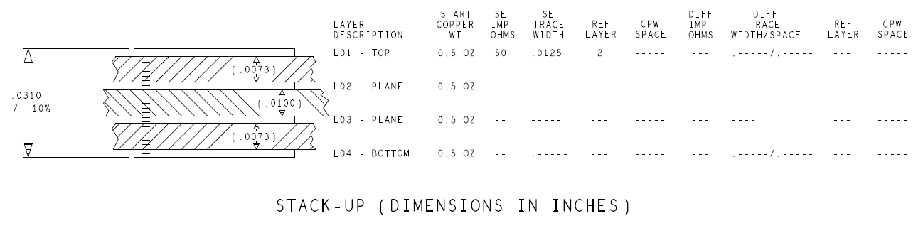
The microstrip used in this reference design is on layer 1 with a trace width of 12.5 mils. The reference ground is layer 2.
This reference design uses a four‐layer PCB with a stackup as shown in Figure 1:
- Layer 1: Components and main signal layer
- Layer 2: Solid ground layer
- Layer 3: Power signal layer
- Layer 4: Digital signal layer. Additional power signals that could not be routed on layer 3 can be routed here. However, ensure that they do not overlap any of the power signals on layer 3
Component placement
As a rule, follow the receive signal flow from the antenna to the antenna matching and filter circuits, then to the low-noise amplifier (LNA) chip input. Keep radio front end (RF), power management unit (PMU), and baseband (BB) decoupling capacitors next to the CYW20829 pin pads.
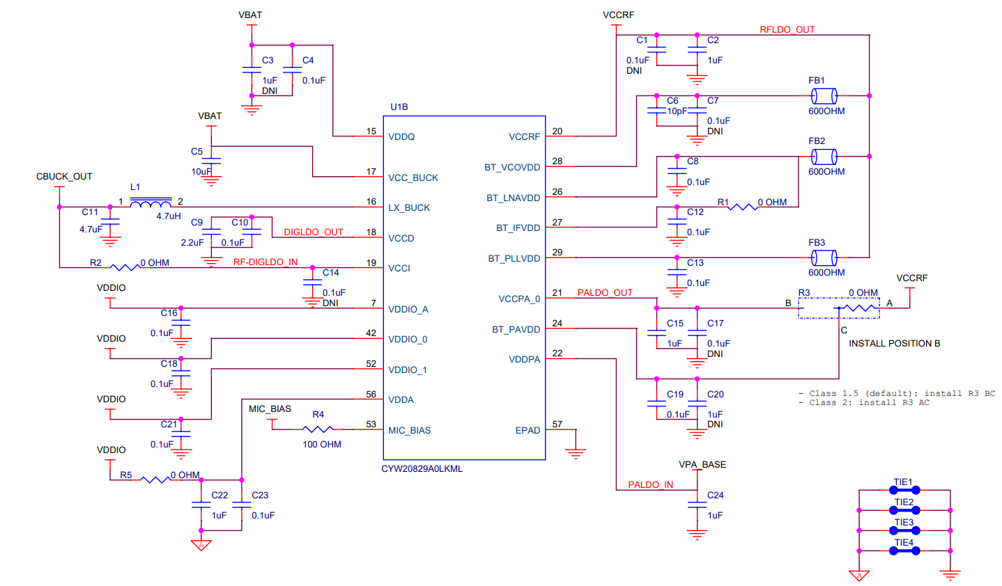
PAVDD supply for CYW20829
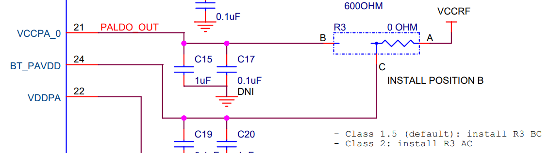
- For CYW20829 Class 1.5, BT_PAVDD must be connected to VCCPA_0 (PALDO_OUT (2.5 V))
- For CYW20829 Class 2.0, BT_PAVDD must be connected to VCCRF (RFLDO_OUT (1.2 V))
Bypass capacitor placement
The following schematic design shows the PMU and the RF front end section. When making determinations about the part placements on the PCB, the following requirements must be met:
- VBAT inputs, which consist of VDDQ (Pin 15) and VCC_BUCK (Pin 17) must have a 0.1-µF (C4) capacitor placed as close to pin 15 as possible and a 10-µF (C5) capacitor placed as close to pin 17 as possible. The second bypass capacitor on VDDQ (Pin 15) is optional and may be omitted if board space is limited
- Both the 4.7-µH (L1) power inductor and 4.7-µF (C11) capacitor must be placed as close to LX_BUCK (Pin 16) as possible
- The bypass capacitor on VCCI (Pin 19) is optional and may be omitted if board space is limited
- VCCD (Pin 18) must have a 2.2-µF capacitor and a 0.1-µF capacitor placed as close to the pin as possible. Place 0.1-µF capacitor closer to the pin
- VCCRF (Pin 20) must have a 1-µF capacitor placed as close to the pin as possible. A second bypass capacitor is optional and may be omitted if board space is limited
- BT_VCOVDD (Pin 28) must have a 10-pF capacitor placed as close to the pin as possible. A second bypass capacitor is optional and may be omitted if board space is limited
- BT_LNAVDD (Pin 26) must have a 0.1-µF capacitor placed as close to the pin as possible
- BT_IFVDD (Pin 27) must have a 0.1-µF capacitor placed as close to the pin as possible
- BT_PLLVDD (Pin 29) must have a 0.1-µF capacitor placed as close to the pin as possible
- VCCPA_0 (Pin 21) must have a 1-µF capacitor placed as close to the pin as possible. A second bypass capacitor is optional and may be omitted if board space is limited
- BT_PAVDD (Pin 24) must have a 0.1-µF capacitor placed as close to the pin as possible. A second bypass capacitor is optional and may be omitted if board space is limited
- VDDPA (PIN 22) must have a 1-µF capacitor placed as close to the pin as possible
In the baseband area, the following component placement must also be met:
- VDDIO_A (Pin 7), VDDIO_0 (Pin 42), and VDDIO_1 (Pin 52) must have a 0.1-µF for each pin, and they must be placed as close to the pin as possible
- VDDA (Pin 56) must have a 0.1-µF capacitor and a 1-µF capacitor be placed as close to the pin as possible
Antenna placement
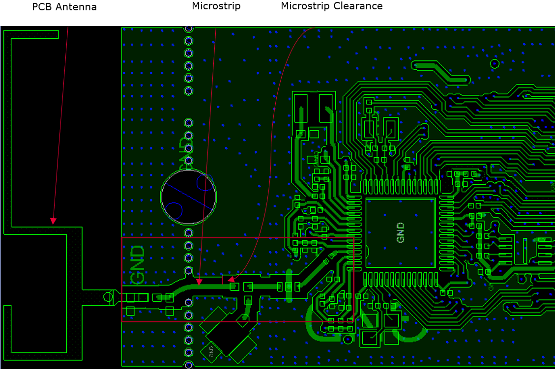
Keep the antenna connection to the device as short as possible. Maintain a solid ground near the antenna and adequate ground clearance for the layers beneath the antenna.
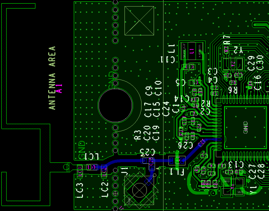
In the reference design, the antenna is on the top layer on the left of the board next to the CYW20829 chip.
For more details on PCB antennas general guideline, see AN91445 - Antenna design and RF layout guidelines. For the associated Gerber file, click here.
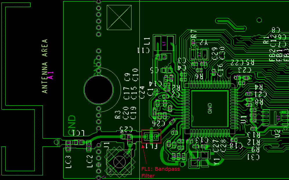
Bandpass filter
Place a chip bandpass filter between the antenna matching components and the CYW20829 device to attenuate harmonics from CYW20829. The chip bandpass filter part used in the CYW20829 reference design is Murata; LFB182G45CL3D178. A microstrip is used for all connections of the bandpass filter. Place a via on the ground pad of the bandpass filter for optimal performance.
Insertion loss and out-of-band attenuation performance depend on PCB component layouts and tolerances. Filter layout should follow general RF layout rules.
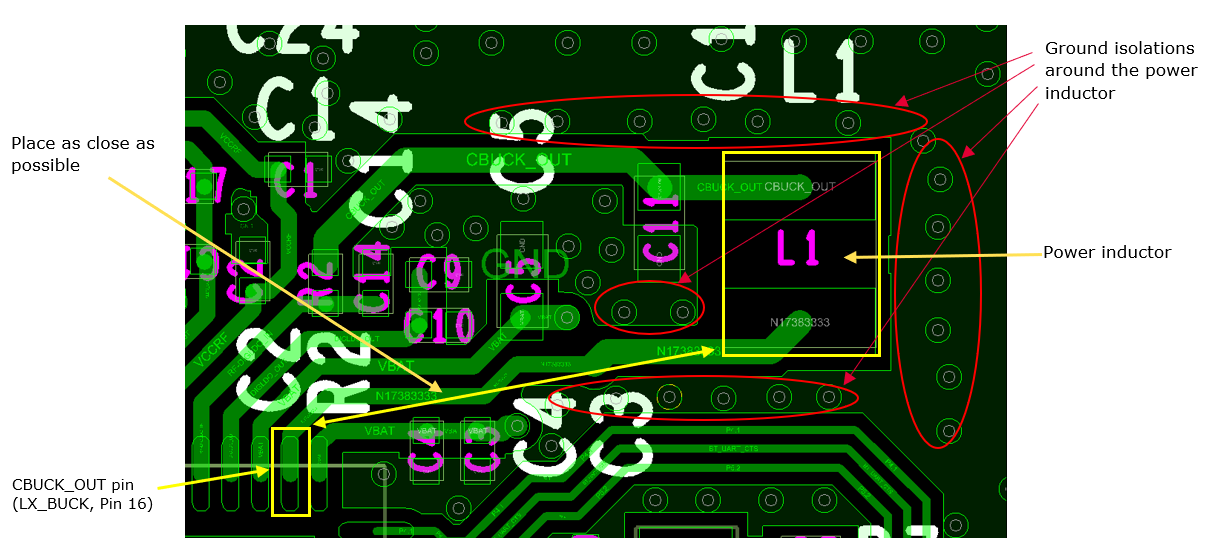
Power inductor placement
The power inductor must have good isolation; this is done by surrounding it with as much ground as possible. The power inductor should also be placed as close to CBUCK_OUT pins (LX_BUCK, Pin 16) as possible. The inductor should be placed adjacent with the output capacitor (C11 in this design). The copper on the PCB top layer under this inductor should be cut out. The power inductor part used in the CYW20829 reference design is Murata; DFE201610E-4R7M=P2
| Parameter | Conditions | Min. | Typ. | Max. | Unit |
|---|---|---|---|---|---|
| External inductor, L1 | 4.7-μH ±20, 1.6A, DCR = 288 mΩ (for frequency < 1 MHz) | - | 4.7 | - | μH |
Crystal specifications and requirements
For the crystal parts, TXC 7R24070007 is recommended for the 24-MHz main crystal, and TAI-SAW TZ3406A for the 32.768-kHz crystal.
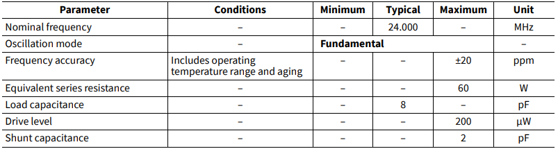
The 24-MHz crystal oscillator must have an accuracy of ±20 ppm as defined by the Bluetooth® specification. Two external load capacitors are required to work with the crystal oscillator. The selection of the load capacitors is XTAL-dependent (see Figure 7).
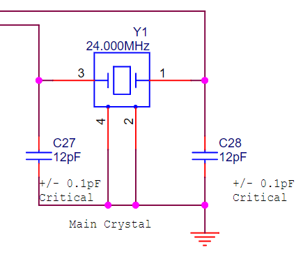
Crystal specifications and requirements for the 24-MHz crystal can be found in Figure 8.
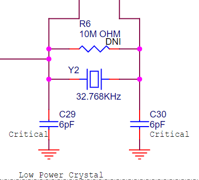
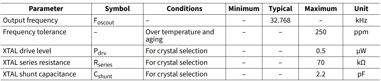
The 32-kHz or 32.768-kHz crystal oscillator must have an accuracy of ±250 ppm or better per the Bluetooth® spec over temperature and including aging. The default component values are: C1 = C2 = ~6 pF. The values of C1 and C2 are used to fine-tune the oscillator. Figure 9 shows the 32 kHz XTAL oscillator with external components and Figure 10 lists the oscillator’s characteristics.
Crystal placement
Protect the crystal and related traces from noise sources and use a solid ground to separate the crystal from RF traces. The crystal ground plane should have direct vias to the reference ground plane.
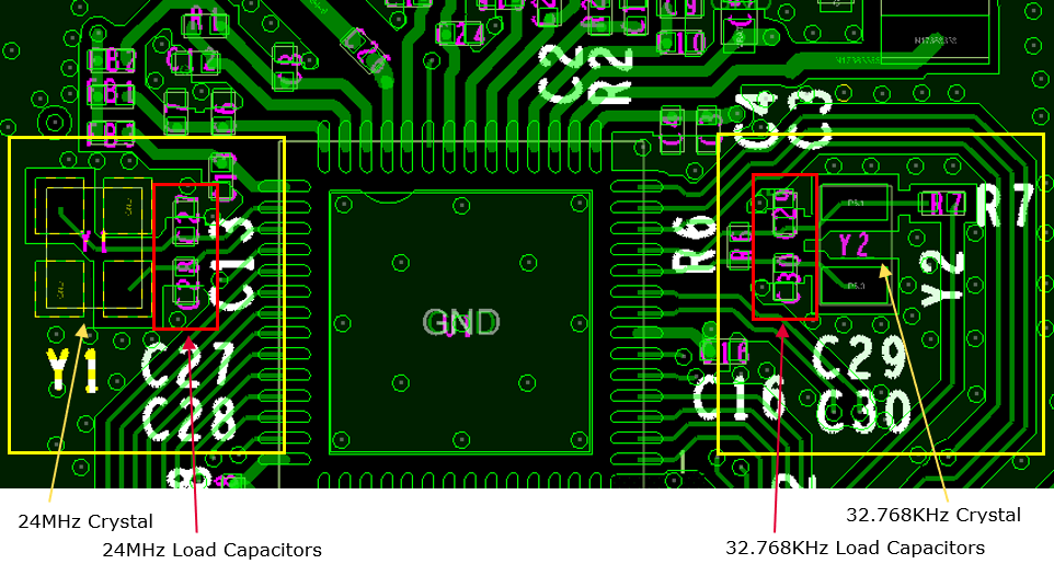
The load capacitors placement as shown in Figure 11 is recommended, because this placement uses the least amount of PCB trace to connect the CYW20829 chip, the crystals, and the crystal load capacitors together which will minimize the parasitic capacitance.
PCB layers and routing
Ground vias
Do not use long thin traces to connect components to ground vias; instead, cover entire ground pad with ground copper and place the ground vias as close to the ground pad as possible. Via on pad is required for the ground pad of the CYW20829. Only use through hole vias in the open area to stitch the ground plane on all layers together. Ensure that there are enough ground pins near the ground pad of the CBUCK output capacitor (C11 in this design).
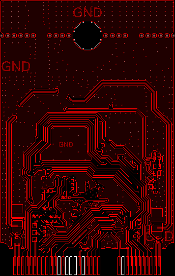
Layer 1: Components, signal fanout, and RF trace
All the passive components for the chip can be placed on the top layer. Signal fanout from the CYW20829 chip will also be done on the top layer.
The RF trace, shown as blue, must be well isolated and have a solid ground plane along both sides of the trace. Ensure that this RF trace is 50-ohm impedance matched.
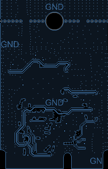
Layer 2: Solid ground plane
Fill the layer immediately below the layer where CYW20829 is located with the solid ground plane for the optimal ground return path.
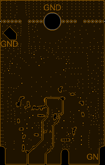
Layer 3: Power traces
- Route the main DC power supply line up the middle of the board like a spine, branching off left and right as needed
- Avoid routing DC power in a loop
- Consider the current flow when routing the power traces to the chip. For input power pins, ensure that the power trace goes through the decoupling capacitors before going into the power pin. For output power pins, ensure that the power trace goes to the decoupling capacitors immediately before going to the load
- Protect the RF power supply from main power, noisy signals, and digital power by separating with ground fill
- Ensure that adequate power trace width and vias are available (or present) to minimize parasitic impedance
- Crossing or overlapping power traces on adjacent layers is not recommended. In the case where power traces crossing cannot be avoided, have them cross in a perpendicular manner to minimize the overlapping area of the power traces. (See the example shown in Section 4.6)
- Recommended Trace width for the power signals are as follows:
- CBUCK_OUT to LX_BUCK (Pin 16) → Minimum 10 mils trace width
- CBUCK_OUT to VCCI (Pin 19) → Minimum 10 mils trace width
- VDDIO → Minimum 10 mils trace width
- VCCD (Pin 18) → Minimum 8 mils trace width
- VBAT to VDDQ (Pin 15)/VCC_BUCK (Pin 17) → Minimum 10 mils trace width
- VCCRF (Pin 20) to BT_VCOVDD (Pin 28)/BT_LNAVDD (Pin 26)/BT_IFVDD (Pin 27)/BT_PLLVDD (Pin 29) → Minimum 8 mils trace width
- VDDPA (Pin 22) to VPA_BASE → Minimum 10 mils trace width
- VCCPA_0 (Pin 21) to BT_PAVDD (Pin 24) → Minimum 8 mils trace width
- MIC_BIAS → Minimum 5 mils trace width
Layer 4: Power traces and non-critical signals
Use layer 4 for all non-critical signal routing and additional power traces that could not be routed on layer 3. Ensure that the power traces routed on layer 4 do not cross with the power traces that are on layer 3.
Unavoidable power trace crossing on adjacent layers
If power traces crossing cannot be avoided, have them cross in a perpendicular manner to minimize the overlapping area of the power traces.
References
A wealth of data is available at www.infineon.com to help you to select the right device, and quickly and effectively integrate the device into your design.
-
Datasheets
-
CYW20829
-
-
Application note
Revision history
| Document revision | Date | Description of changes |
|---|---|---|
| ** | 2022-11-02 | Initial release |
| *A | 2024-04-04 | Updated template; no content update |
Trademarks
The Bluetooth® word mark and logos are registered trademarks owned by Bluetooth SIG, Inc., and any use of such marks by Infineon is under license.