This application note introduces the CAPSENSE™
multi-sense converter (MSC) block of PSOC™ HV mixed signal (MS)
family MCUs. This application note also describes how to develop hardware and firmware
design for human machine interface (HMI), body, and powertrain
applications.
Intended audience
The intended audience for this document is design engineers,
technicians, and developers of electronic systems.
Introduction
PSOC™ HVMS is a fully integrated programmable embedded
system for several automotive HMI, body, and powertrain applications. The system features
an Arm®
Cortex® M0+ processor with programmable and reconfigurable analog and
digital blocks. It is a combination of a microcontroller with a 12-bit SAR ADC,
5th-generation multi-sense converter (MSC) block supporting capacitive sensing (CAPSENSE™), digital peripherals such as PWMs and serial communication
interfaces along with a LIN interface with integrated PHY, and a high-voltage subsystem to
operate directly off the 12 V car battery.
PSOC™ HVMS is available in a
32-/48-/56-/64-QFN package with wettable flanks. To understand the functionality described
and terminology used in this application note, see the Overview section of the architecture
reference manual and AN185951 - PSOC™ 4
and PSOC™ 6 MCU CAPSENSE™ design guide. See References in this application note for more details.
Multi-sense converter overview
The multi-sense converter (MSC) is supported on all pins in PSOC™ HV MS via MSC CAPSENSE™ block that can be connected to
any pin via the analog MUX buses that any GPIO pin can be connected to. The MSC block in
the PSOC™ HVMS can be used to scan sense inputs autonomously (without
CPU sequencing and intervention) with support for DMA or can operate via CPU
firmware-driven switch sequencing via the analog MUX buses that any GPIO pin can be
connected to. The CAPSENSE™ function can thus be provided on any pin or
group of pins in a system under software control.
The MSC block supports the following;
One MSC converter
Both self-capacitance (CSD) and mutual-capacitance (CSX) sensing
Multi-sense (capacitive, resistive, impedance, and current sensing)
Support 5:1 or more signal-to-noise ratio (SNR) and water tolerance
Autonomous scanning (scan multiple sensors without CPU involvement)
Improved water tolerance (uses both passive and active shields)
The CAPSENSE™ blocks provide both self as well as
mutual capacitance sensing. Shield drive can be either active (with an opamp) or passive
(less power, for shield loads less than 20 pF).
Figure 1 shows the MSC CAPSENSE™ block diagram. The main features include ratio-metric sensing,
differential mode of operation without the need of reference voltage, use of capacitor DACs
(CDAC) in place of current DACs (IDAC) which improves noise performance.
Figure 1. MSC CAPSENSE™ block diagram
GPIO cell capacitance to charge converter
In the MSC architecture, the sensor is either interfaced to the AMUX or a
new control MUX matrix, which supports autonomous scanning (limited number of pins
supported). The GPIO cells are configured as switched-capacitance circuits that convert
sensor capacitances into equivalent charge transfer. Figure 2 shows the GPIO cell structure.
Figure 2. GPIO cell structure
Four non-overlapping, out-of-phase clocks of frequency FSW control the
switches (SW1, SW2, SW3, and SW4) as Figure 3
shows.
Figure 3 shows
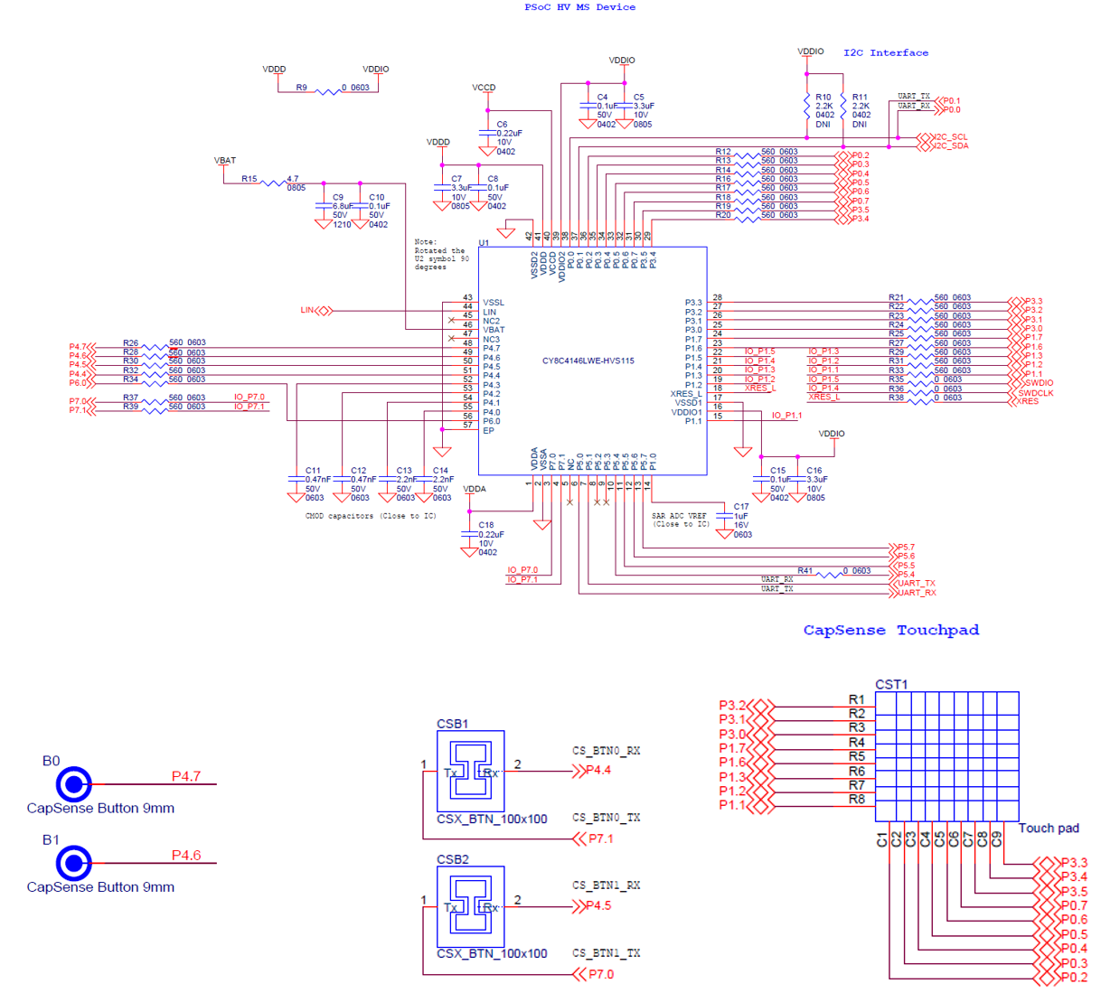
a general schematic of an external circuit (2x CSD buttons, 2x CSX buttons, and 1x
touchpad) for the MSC block of the PSOC™ HVMS MCU. See
AN234116 - Hardware design guide in References for
more information of the power block.
Figure 4. General schematic for MSC block
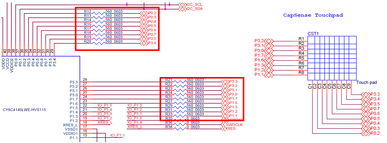
Series resistors on CAPSENSE™
pins
Every CAPSENSE™ controller pin has some parasitic
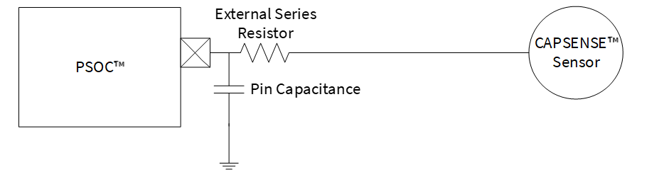
capacitance (CP) associated with it. As Figure 5 shows, adding an external resistor forms a
low-pass RC filter that attenuates the RF noise amplitude coupled to the pin. This
resistance also forms a low-pass filter with the parasitic capacitance of the CAPSENSE™ sensor that significantly reduces the RF emissions.
Figure 5. RC filter
Series resistors should be placed close to the device pins so that the radiated noise picked by the traces gets filtered at the input of the device. Thus, it is recommended to place series resistors within 10 mm of the pins.
For CAPSENSE™ designs using copper on PCBs, the
recommended series resistance for CAPSENSE™ input lines are 560 Ω.
Adding resistance increases the time constant of the switched-capacitor circuit that
converts CP into an equivalent resistor. If the series
resistance value is larger than 560 Ω, the slower time constant of the switching circuit
suppresses the emissions and interference but limits the amount of charge that can
transfer. This lowers the signal level, which in turn lowers the SNR. Smaller values are
better in terms of SNR, but are less effective at blocking RF.
CAPSENSE™ buttons
Schematic example
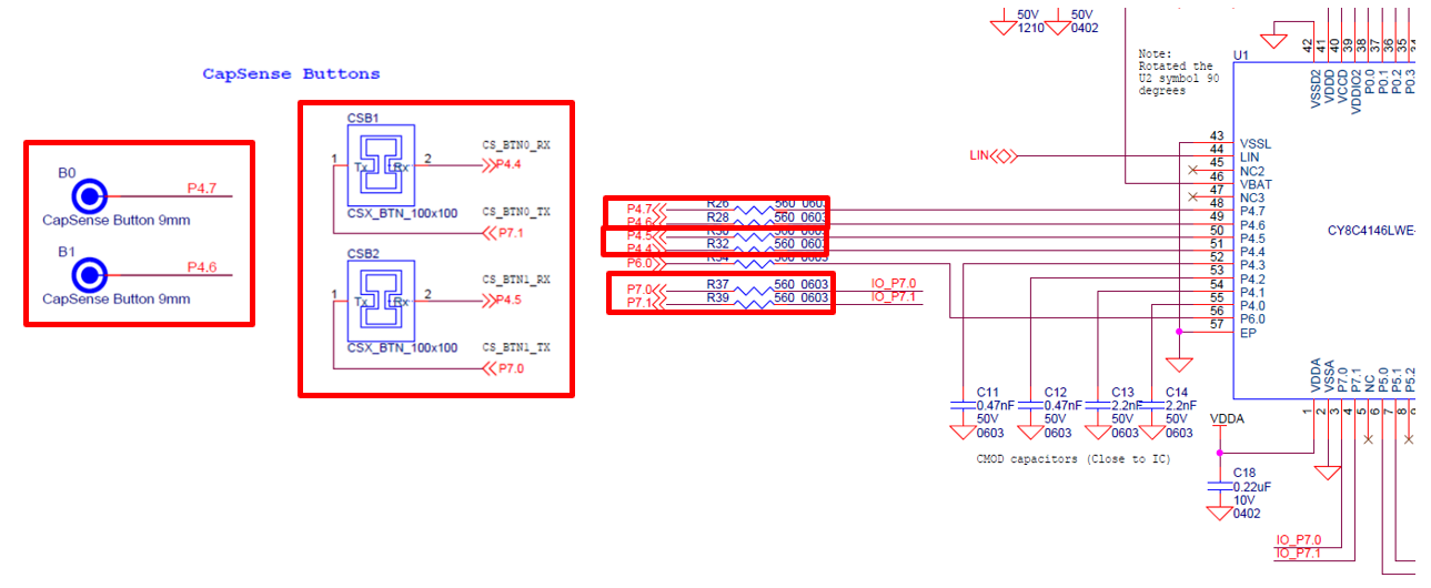
This example (Figure 6) is using 2x
CSD buttons (round solid) and 2x CSX buttons (fishbone patterns). The feature of each
button is:
CSX button: High sensitivity, high noise tolerance, and allow multiple buttons without ghost effect
B0 and B1 are connected to P4.7 and P4.6 GPIOs. CSB1 is connected to P7.1 (TX) and P4.4 (RX) GPIOs, and CSB2 is connected to P7.0 (TX) and P4.5 (RX) GPIOs.
Note: The MSC block of PSOC™ HVMS can be connected to all GPIO pins via the analog MUX buses.
Table 1. External component example for CAPSENSE™
buttons
Symbol
Overview
Parameter
Value 1
Value 2
Value 3
B0, B1
CSD button
round solid
9 mm
-
CSB1, CSB2
CSX button
fishbone pattern
10 x 10 mm
-
R26, R28, R30, R32, R37, R39
Series resistor
560 Ω
+/- 1%
> 1/10 W
Layout example
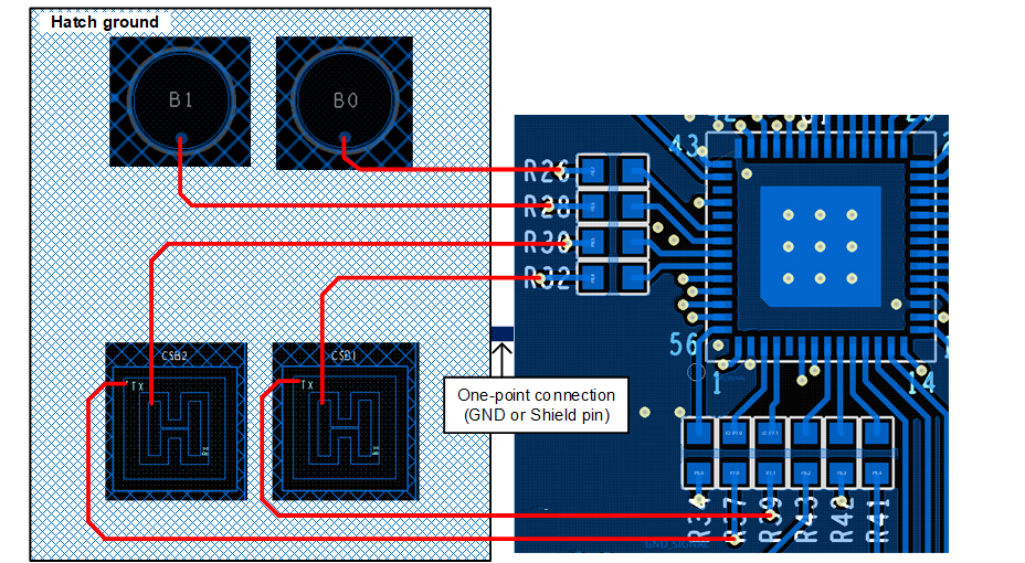
Figure 7 shows an example of CSD and
CSX button layout.
Note:
PSOC™ HVMS silicon is placed on top side in this
example.
Red lines mean the bottom side.
Figure 7. Layout example of CSD and CSX buttons
Follow these guidelines for the design of the CAPSENSE™
button circuit on the PSOC™ HV MS:
Place the external series resistors near the IC terminal
Draw the CAPSENSE™ lines on the bottom side (If
possible, also place the PSOC™ HV MS silicon on the bottom
side)
Create the hatch ground around CAPSENSE™ buttons
(See AN85951 for more detailed hatch ground)
Divide the ground plane between shape ground and hatch ground using one-point connection (GND or shield pin)
To avoid a cross-talk, each CAPSENSE™ line has to
follow the 3 W rule states that “to reduce cross talk from adjacent traces, a minimum
spacing of two trace widths should be maintained from edge to edge”
For CSX buttons, use different GPIO ports for Tx and Rx pins (e.g., TX: port 7, Rx: port 4)
Provide a through-hole (via) for the CAPSENSE™
button on the edge of each button
Recommend that the final finish is electroless nickel/immersion gold (ENIG)
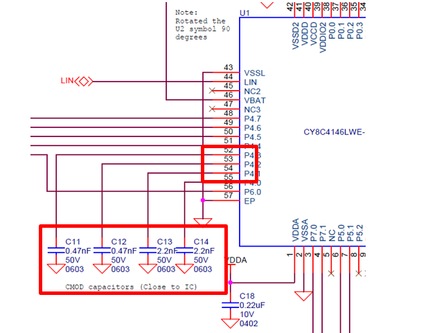
CMOD capacitors
Schematic example
The sigma-delta converter in MSC block uses an external integrating
capacitor, called a modulator capacitor CMOD. Figure 8 shows the CMOD capacitor
connection for the PSOC™ HV MS family.
Note:
The CMOD value of PSOC™ HV MS supports up to 10
nF and typical is 2.2 nF.
Increasing CMOD have the adverse effect of increasing the noise,
initialization time, and minimum signal required to detect.
MSC method requires two external integration capacitors, CMOD1 and
CMOD2.
C13 and C14 are typically used. C11 and C12 are optional.
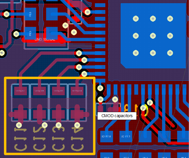
Follow these guidelines for the design of the CMOD capacitor circuit on the PSOC™ HV MS:
Place the CMOD capacitors near the IC terminal
If the CMOD capacitors are placed in a different layer of PCB, provide a through-hole (via) near the IC terminal
Provide a ground through-hole near this capacitor to minimize the current loop
Place the GND layer under the CMOD capacitors
CAPSENSE™ touchpad
Schematic example
This example (Figure 10) is using a 9
× 8 touchpad (also known as trackpad). The touchpad has two linear sliders arranged in an X
and Y pattern, enabling it to locate a finger’s position in both X and Y dimensions. The
touchpads can be sensed using either CSD or CSX sensing method.
CSD-based touchpads suffer from ghost touches, so it supports only single-point touch applications.
CSX touchpads can support multi-point touch applications, but these may need more scanning time compared to the CSD touchpad because this method scans each intersection rather than rows and columns.
Figure 10. Schematic example of CAPSENSE™ touchpad
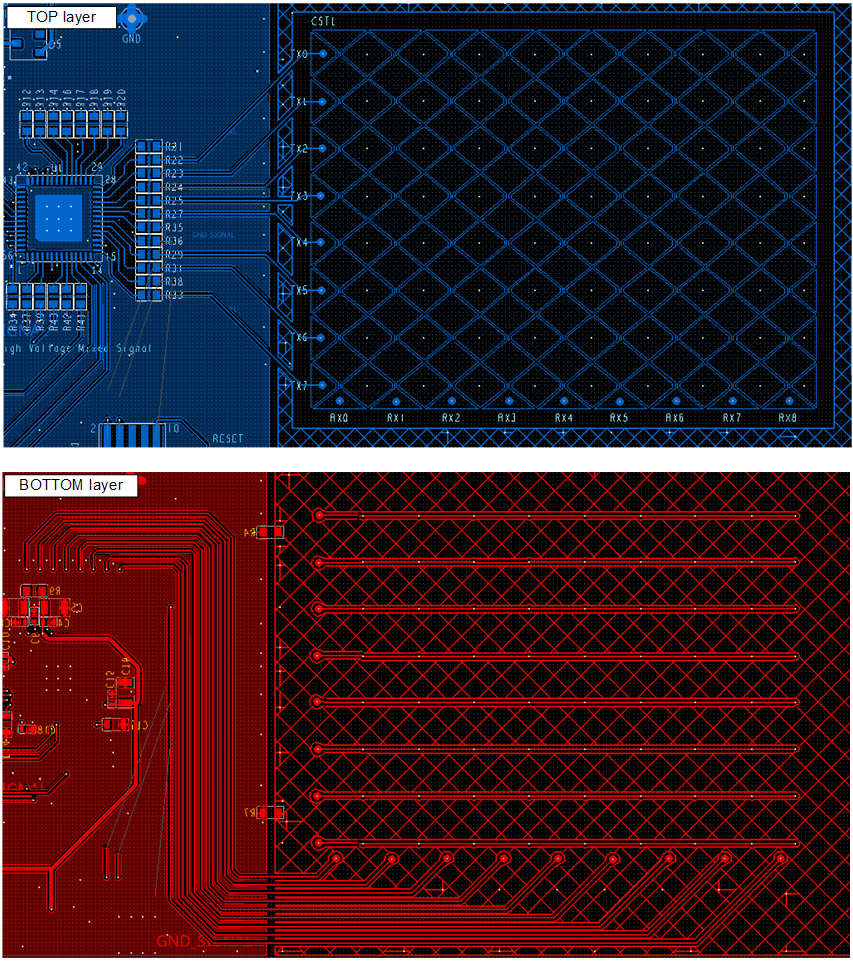
PSOC™ HV MS silicon is placed on top side in this
example.
Blue color is the top layer and red color is the bottom layer.
Figure 11. Layout example of touchpad
Follow these guidelines for the design of the touchpad circuit on the PSOC™ HV MS:
Place the external series resistors near the IC terminal
Draw the touchpad lines on the bottom side (If possible, also place the
PSOC™ HV MS silicon on the bottom side)
Create the hatch ground around the touchpad (See AN85951 for more detailed hatch ground)
Divide the ground plane between shape ground and hatch ground using one-point connection (GND or shield pin)
To avoid a cross-talk, each trackpad line has to follow 3 W rule states
If possible, enter a ground guard into each trackpad line
Connect the lines to the edge of the touchpad shape using the through-hole
Recommend of final finish is electroless nickel/immersion gold (ENIG)
AutoPDL firmware configuration
Infineon provides an evaluation license of the Automotive Peripheral Driver
Library (AutoPDL) including startup code as sample firmware. The AutoPDL provides the
low-level drivers for all PSOC™ HV peripherals with ISO 26262
compliant. The following features of AutoPDL are available.
Drivers and middleware
Low-level drivers for all peripherals
Middleware for complex peripherals such as CAPSENSE™
Quality ASPICE Level 2
MISRA 2012 AMD1, CERT C “Rules” (L1, L2, L3) are applied,
Deviations/Warnings documented.
Traceability
Safety ASIL-B
Safety documentation reduces customers’ effort for safety
qualification.
Safety features based on SEooC.
Compiler version
IAR Embedded Workbench for Arm®, Functional
Safety, version 8.50
Note:
CAPSENSE™ firmware configuration is created based on AutoPDL version
1.3.1.
CAPSENSE™ middleware
The middleware is a set of firmware drivers that provide APIs for accessing the hardware. These APIs perform the initialization and control activities of each peripheral.
Table 4 lists and describes the
interface to each CAPSENSE™ function. The peripheral drivers of CAPSENSE™ are located in the AutoPDL path of:
<user path>\source\middlewares\capsense\src
Note: The CAPSENSE™ has many
registers to configure it (provide the hardware drivers as a binary file). Table 4 is simplified to only expose the controls the
customer should be using. For more detailed information, see UsersGuide_Capsense
_x_x_PSoC4HV_PDL.pdf in <user path>\doc folder.
Table 4. CAPSENSE™ functions
Function
Description
cy_cs_functions.h
Cy_Cs_Init()
Captures MSC HW block for CAPSENSE™
operations and configures it to the default state.
Cy_Cs_DeInit()
Stops the CAPSENSE™ middleware
operation, releases the captured MSC hardware block, and resets all assigned
GPIO sensing pins to the HI-Z analog driving mode.
Cy_Cs_Enable()
Enables the MSC HW block and its interrupt.
Cy_Cs_Disable()
Disables the MSC hardware block, its assigned clock divider, and interrupt.
Cy_Cs_InitAllWidgets()
Calibrates widgets that have Cref = Cfine = 0 values in the configuration, initializes baselines for all widgets, and executes the BIST.
Cy_Cs_CalibrateWidget()
Executes CapDAC auto-calibration for the specified widget.
Cy_Cs_CalibrateAllWidgets()
Executes CapDAC auto-calibration for all widgets.
Cy_Cs_GetWidgetCalAcc()
For the specified widget, calculates the maximum deviation of the sensor scan data from the calibration target in percent.
Cy_Cs_InitWidgetBaselines()
Executes a full scan and initializes baselines for the specified widget.
Cy_Cs_InitAllBaselines()
Executes a full scan and initializes baselines for all the widgets.
Cy_Cs_ScanWidget()
Initiates the scanning of all sensors in the specified widget. All supported by the widget scan types, i.e., CSD, CSX, and Listening will be performed. Scanning is initiated only if no scan is in progress. Scan finishing can be checked by the Cy_Cs_IsBusy() function.
Cy_Cs_BlockingScanWidget()
Initiates the scanning of all sensors in the specified widget and waits until the scan is done. All supported by the widget scan types, i.e., CSD, CSX, and listening will be performed. Scanning is initiated only if no scan is in progress.
Cy_Cs_ScanAllWidgets
Initiates the scanning of all widgets. All supported by each widget scan types, i.e., CSD, CSX, and Listening will be performed. Scanning is initiated only if no scan is in progress. Scan finishing can be checked by the Cy_Cs_IsBusy() function.
Cy_Cs_IsBusy()
This function returns the status of the CAPSENSE™ middleware whether a scan is currently in progress or
not.
Cy_Cs_GetScanStatus()
Returns the error code of the latest scan.
Cy_Cs_ProcessWidget()
Performs full data processing of the specified widget.
Cy_Cs_ProcessAllWidgets()
Performs full data processing of all the widgets.
Cy_Cs_GetWidgetTouchStatus
Reports whether the specified widget detected touch on any of its sensors.
Cy_Cs_GetTouchReport()
Returns a pointer to the touch report structure.
Cy_Cs_SetTimeStamp()
This function writes the specified value into the middleware internal timestamp register that is used for gesture detection.
Cy_Cs_IncrementTimeStamp()
Increments the timestamp register by the preconfigured CY_CS_CFG_TIMESTAMP_INTERVAL value.
Cy_Cs_DecodeWidgetGestures()
Performs decoding of all enabled gestures for the specified widget.
Cy_Cs_GetWidgetNoiseLevel()
Returns normalized noise level for the specified widget. The noise level is expressed in percent, 100% corresponds to the noise data equal to the CY_CS_CFG_WDx_NOISE_THRESHOLD configuration parameter.
Cy_Cs_GetMaxNoiseLevel()
Returns the maximum normalized noise level of all widgets. The noise level is expressed in percent.
Cy_Cs_RunSelfTest()
Runs built-in self-tests that are specified by the test enable mask parameter.
Cy_Cs_GetCpValue()
Calculates the self-capacitance (CSD) value for the specified sensor.
Cy_Cs_GetCmValue()
Calculates the mutual capacitance (CSX) value for the specified Tx/Rx sensors crossing.
Cy_Cs_GetBistData()
Returns a pointer to the built-in self-test results structure.
Cy_Cs_SetCallbackTunerSendData()
Registers a user's callback function for data transmission.
The registered function will be called by the CAPSENSE™
middleware to initialize a data transmission to the tuning application. This
function must be called prior to Cy_Cs_InitTuner() call.
Cy_Cs_SetCallbackTunerRdCmplt()
Registers a user's callback function for checking if the
previous report transmission is finished. The registered function will be
called by the CAPSENSE™ middleware before sending a new
report to the tuning application. If the previous data transmission is not
finished, the new reports will be delayed or skipped. This function must be
called prior to Cy_Cs_InitTuner() call.
Cy_Cs_InitTuner()
Initializes the tuner.
Cy_Cs_ProcessTunerReport()
Creates and transmits the tuning reports. It should be called after processing all the widgets. This function can be blocked if the previous report transmission is not finished or the report size is bigger than the communication buffer. Otherwise, the report transmission is done in the background.
Cy_Cs_GetContext()
Returns a pointer to the middleware context structure. It can be used to access all available data structures.
AutoPDL code example
The following items are required to successfully execute the CAPSENSE™ examples.
Evaluation kit (CYHVMS-64K-56-001 or KIT_PSOC4-HVMS-64K_LITE)
IAR EWARM 8.50.9 (or FS 8.50.10)
AutoPDL evaluation lisence or source code
PSoCAutomotiveConfigurationTool software GUI tool
AutoPDL comes with three examples for using these different types of
widgets (sliders, buttons, and touch pad). The user can either select one of these three
CAPSENSE™ configuration files that are already made part of the
“<user path>\examples\capsense\usercfg” and its corresponding
.csproject file.
Note: KIT_PSOC4-HVMS-64K_LITE kit only supports “CSX_buttons.csproject”.
CAPSENSE™ MW demo
application
Before starting the demo application, connect the power supply and any cables to the evaluation kit. See the relevant user guides for more details.
CAPSENSE™ middleware demo
application is in the following AutoPDL folder.
<user path>\examples\capsense
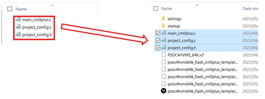
Go to the CAPSENSE™ example folder and copy the
following files.
main_cm0plus.c
project_config.c
project_config.h
Navigate to the following path and replace/paste the copied files into
the folder as shown in Figure 12.
<user path>\examples\Tools\psoc4hvms64k(or
128k)Figure 12. Replacing the header and code files
Run the IAR EWARM 8.50.xx tool.
Open the IAR project file of psoc4hvms64k (or
128k)_flash_cm0plus_template.eww in the
examples\Tools\psoc4hvms64k(or 128k) folder.
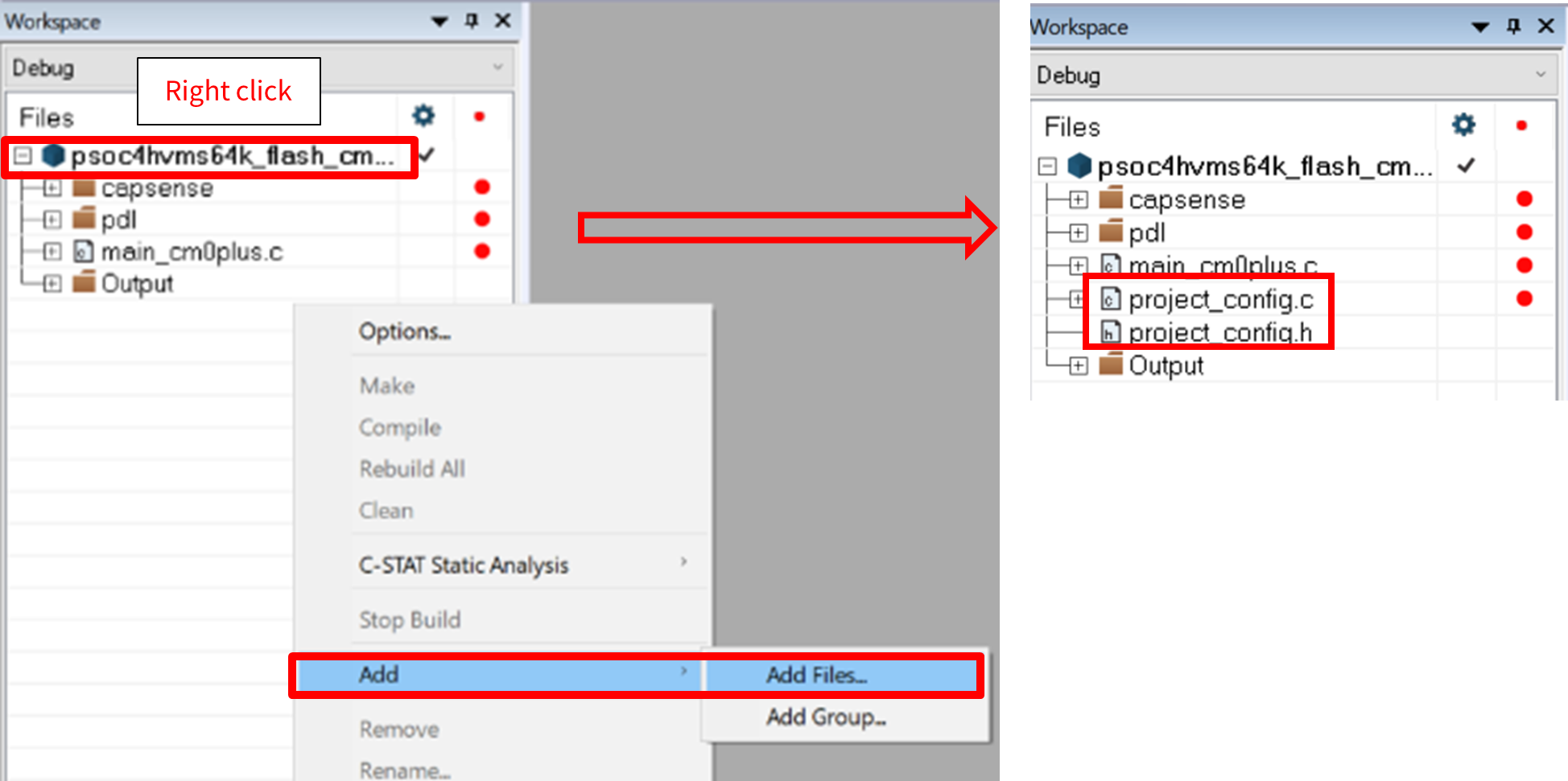
Click psoc4hvms64k (or
128k)_flash_cm0plus_template.eww on the Debug window, right-click,
select Add > Add Files and select the pasted project_config.c and project_config.h files from the examples\Tools\psoc4hvms64k(or 128k) folder.Figure 13. Debug window preview
Select Project > Rebuild All.
The build is completed when the following message is displayed. Figure 14. Build complete preview
Download the application (Project > Download > Download active application) and push the reset switch on the evaluation board.
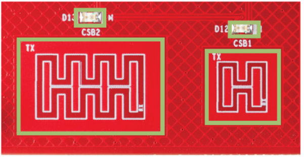
For the CYHVMS-64K-56-001 evaluation board, touch the CSB1 or CSB2
buttons to confirm the CAPSENSE™ operation and observe the
corresponding LED (D12 or D13) lights up.Figure 15. CYHVMS-64K-56-001 Evaluation Board
PSOC™ Automotive configuration tool
Open PSoCAutomotiveConfigurationTool.exe
(Windows Start menu > Infineon Technologies).
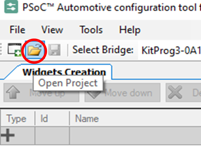
Click Open Project in the upper left toolbar.Figure 16. Click Open Project in the toolbar
Select the CSX_buttons.csproject file from the
following path.
<user path>\examples\capsense\usercfg
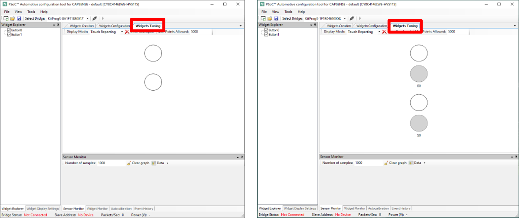
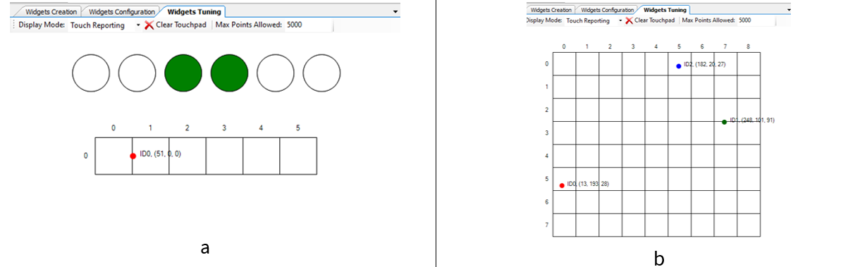
Select the Widgets Tuning tab. One of the
following windows appears.Figure 17. Widgets Tuning tab
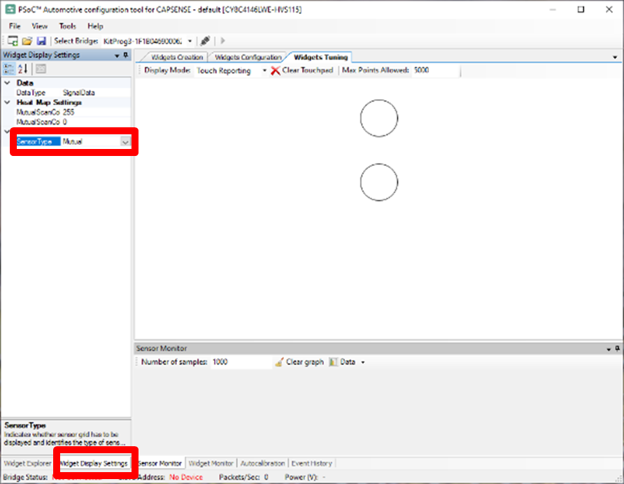
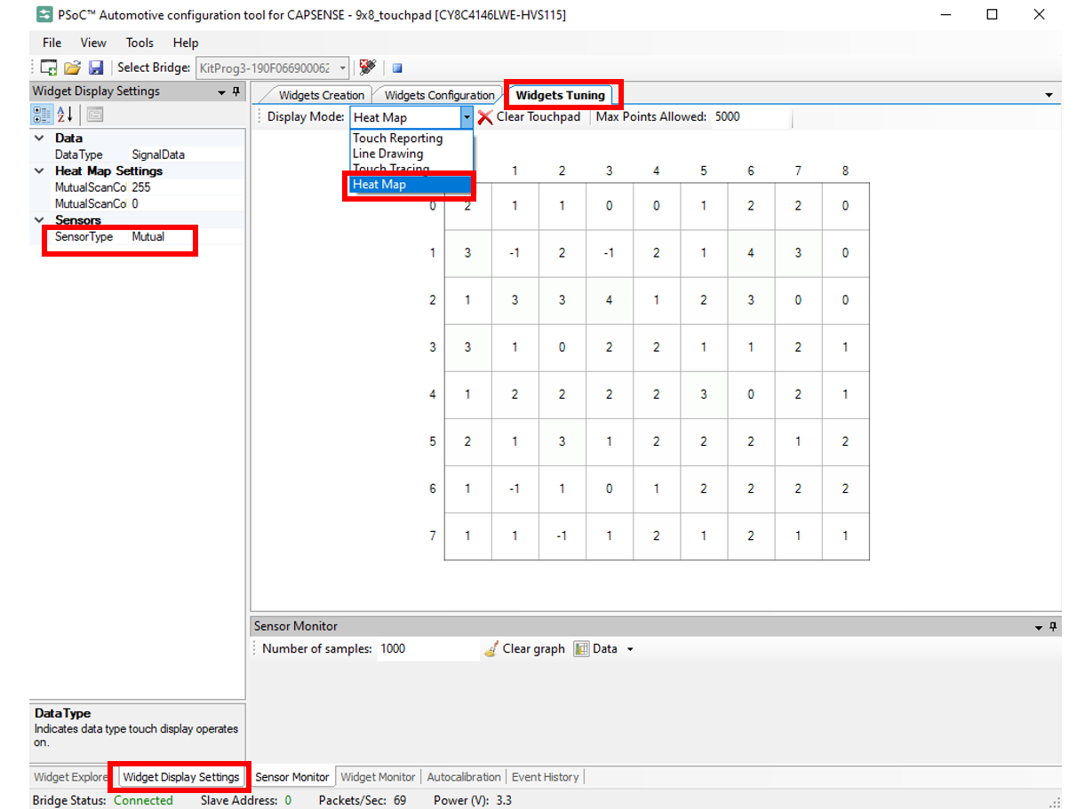
Select the Widget Display Settings tab that is
located on the bottom side of the tool. Ensure that the Sensor Type =
Mutual.Figure 18. Widget Display Settings tab
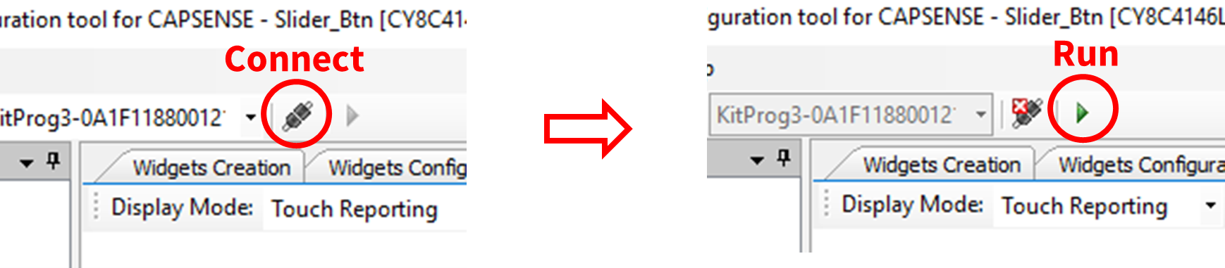
Click Connect, and then click Run.
If the connection is not working, disconnect and reconnect the wall adapter and USB
cable.
Figure 19. Click Connect, and then click Run
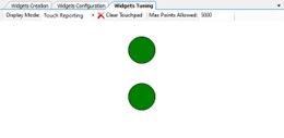
Touch the CAPSENSE™ CSB1 or CSB2 buttons.
You can observe the touching status on the tool.
Figure 20. Touching status on the tool
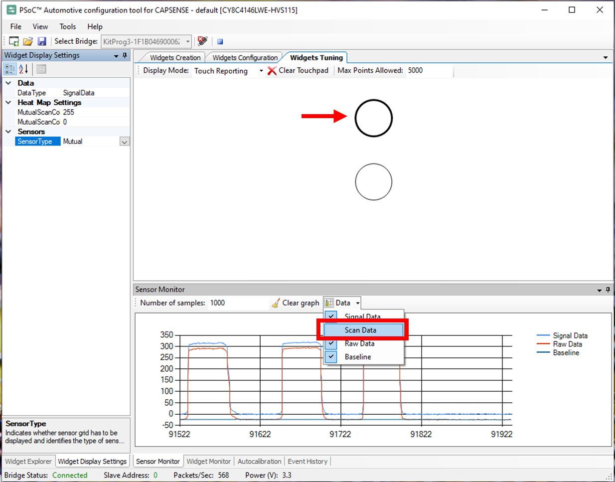
Click the white circle to show the waveform of the sensor. Select the
Data drop down menu and unselect Scan
Data. You can observe the CAPSENSE™ waveform in the
Sensor Monitor window.Figure 21. Sensor Monitor window
CAPSENSE™ slider and touchpad demo
application
Note: For the KIT_PSOC4-HVMS-64K_LITE kit, the slider and touchpad board are not included in the kit. Skip these steps when you use the kit.
Close and open
PSoCAutomotiveConfigurationTool.exe (windows start menu > Infineon Technologies).
Click Open Project.
Select Slider_Btn.csproject or
9x8_touchpad.csproject.
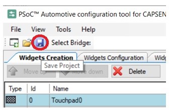
Click Save Project to generate the
cy_cs_cfg.h file in the same folder as the
xxx.csproject path.Figure 22. Click Save Project in Widgets Creation tab
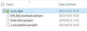
Confirm the cy_cs_cfg.h file with
updated Date modified.Figure 23. Update Date modified
Connect either extension board (slider or touchpad) to
CYHVMS-64K-56-001 evaluation board. Note that KIT_PSOC4-HVMS-64K_LITE is not included in
the extension board.
Open IAR project file of psoc4hvms64k(or
128k)_flash_cm0plus_template.eww.
Select Project > Rebuild All.
Download the application (Project > Download > Download active application) and push the reset switch on the evaluation board.
Touch extension board buttons, slider, or touchpad. The location you
are touching is displayed on the PSoCAutomotiveConfigurationTool.
Note: To show the wave form of each data,
select the Widget Display Settings tab that is located on the bottom
side of the tool. Change the Sensor Type = Self.
After the sensor layout is complete (see Schematic and layout example and PCB layout guidelines
of AN85951), the next step is to implement the firmware and tune
the CAPSENSE™ parameters for the sensor to achieve optimum performance.
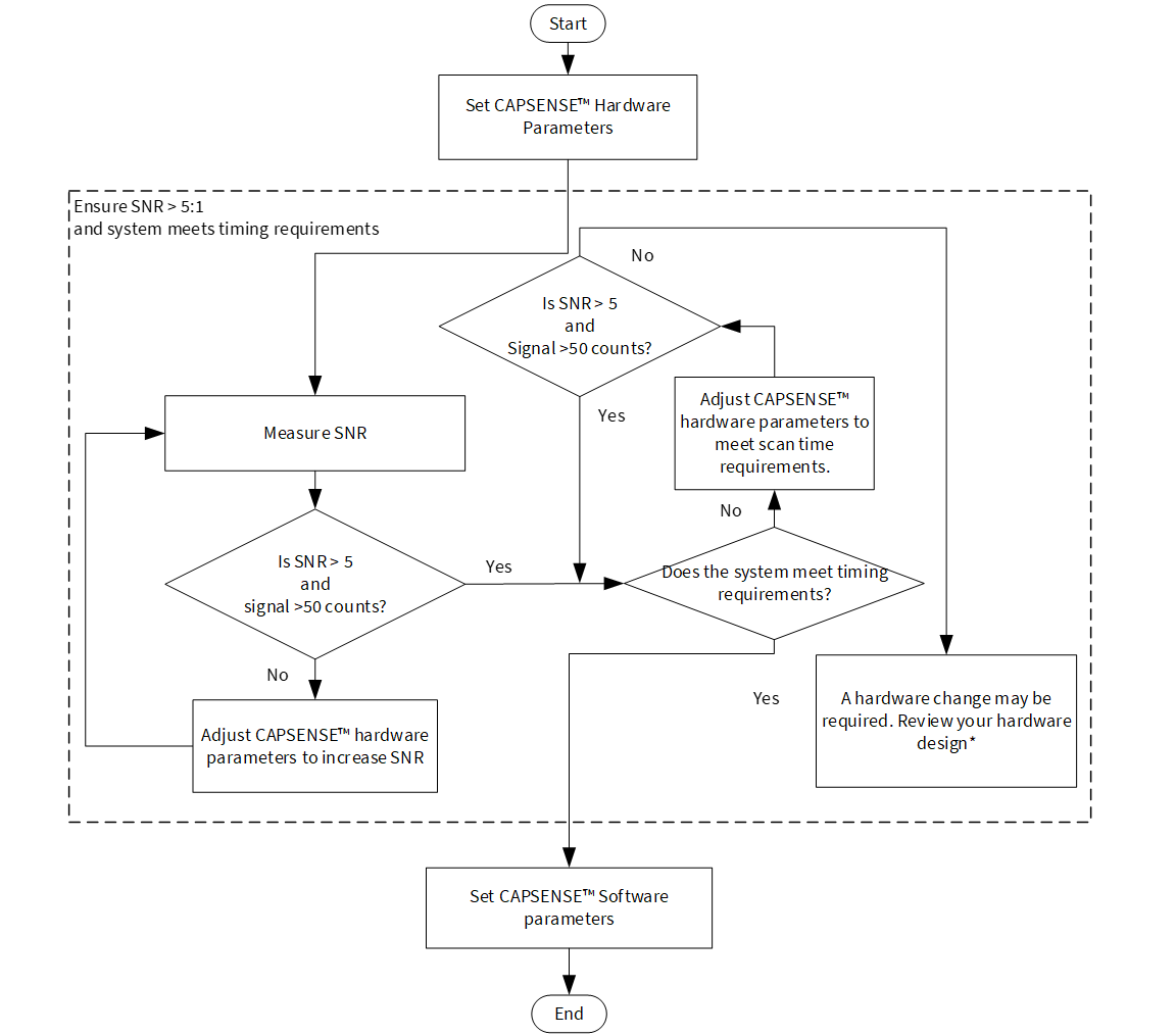
The CAPSENSE™ sensing method is a combination of hardware and firmware
techniques. Therefore, it has several hardware and firmware parameters required for proper
operation. These parameters should be tuned to optimum values for reliable touch detection
and fast response. Most of the capacitive touch solutions in the market must be manually
tuned. Figure 25 shows a general manual tuning
procedure.
Figure 25. Manual tuning process overview
Signal-to-noise ratio (SNR)
In practice, the raw counts (equivalent digital counts) vary due to inherent
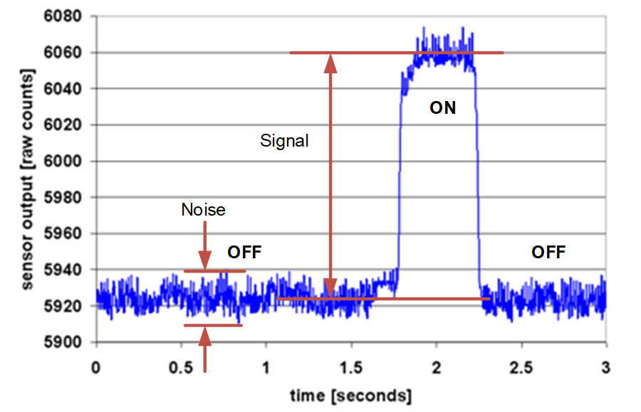
noise in the system. CAPSENSE™ noise is the peak-to-peak variation in
raw counts in the absence of a touch, as Figure 26
shows.
A well-tuned CAPSENSE™ system reliably discriminates
between the ON and OFF states of the sensors. To achieve good performance, the CAPSENSE™ signal must be significantly larger than the CAPSENSE™ noise. SNR is defined as the ratio of CAPSENSE™
signal to CAPSENSE™ noise is the most important performance parameter
of a CAPSENSE™ sensor.
Figure 26. Signal-to-noise ratio (SNR)
In this example, the average level of raw count in the absence of a touch is
5925 counts. When a finger is placed on the sensor, the average raw count increases to 6060
counts, which means the signal is 6060 – 5925 = 135 counts. The minimum value of the raw
count in the OFF state is 5912 and the maximum value is 5938 counts. Therefore, the CAPSENSE™ noise is 5938 – 5912 = 26 counts. This results in an SNR of
135 / 26 = 5.2.
The minimum SNR recommended for a CAPSENSE™ sensor is 5.
This 5:1 ratio comes from best practice threshold settings, which enable enough margin
between signal and noise to provide reliable ON/OFF operation.
Note: Typical application requires a minimum 5:1 SNR, but better to have above 10:1 if EMC and temperature variation issues are expected.
CSD button tuning
This section explains how to tune the self-capacitance-based button manually for optimum performance with respect to parameters such as reliability, power consumption, response time, and linearity using the CSD-RM sensing technique and PSoCAutomotiveConfigurationTool. Here, capacitive sigma-delta (CSD) represents the self-capacitance sensing technique and RM represents the ratio-metric method.
Note: For the KIT_PSOC4-HVMS-64K_LITE kit, the CSD-RM board is not included in the kit. Skip the CSD button-tuning section when you use the kit.
Measure the parasitic capacitance
(CP)
The capacitance of the sensor in the absence of a touch is called the
parasitic capacitance, CP. CP results
from the electric field between the sensor (including the sensor pad, traces, and vias) and
other conductors in the system such as the ground planes, traces, and any metal in the
product’s chassis or enclosure. The GPIO and internal capacitances of PSOC™ also contribute to the parasitic capacitance. However, these internal
capacitances are typically very small when compared to the sensor capacitance.
Connect the CSD liner slider extension board to
the CYHVMS-64K-56-001 evaluation board. Note that KIT_PSOC4-HVMS-64K_LITE is not
included in the extension board.
Open 1x_CSD_button.csproject on
PSoCAutomotiveConfigurationTool.exe.
Click Save Project button to generate
cy_cs_cfg.h file in the same folder as the
xxx.csproject path.
Download the application on IAR EARM.
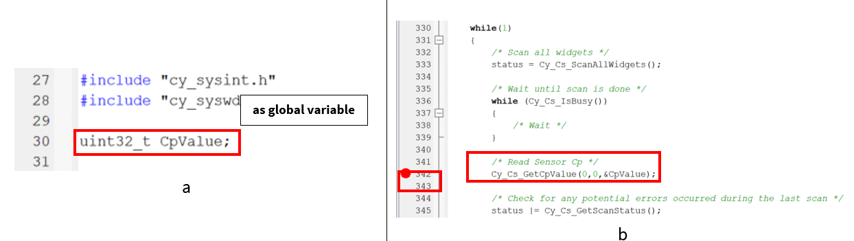
Estimate the CP of the sensor electrode
using the Cy_Cs_GetCpValue() function in the firmware. The measured capacitance value is
in femtofarad (fF).
Add the following code in main_cm0plus.c
and add the breakpoint into code line of Cy_Cs_GetCpValue() function.Figure 27. uint32_t CpValue (a), Cy_Cs_GetCpValue(0, 0, &CpValue) (b)
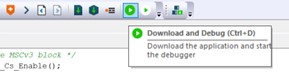
Click Download and Debug button.Figure 28. Download and Debug button
Double-click the CpValue, and right-click to show the menu. Select Add
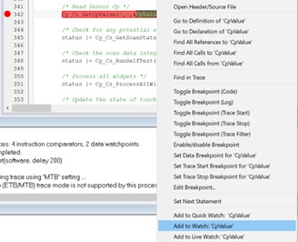
to Watch: ‘CpValue’.Figure 29. Add to Watch: ‘CpValue’ preview
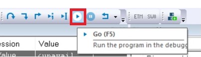
Click Go to run the debugging.Figure 30. Run debugging
Monitor CP value in fF.Figure 31. Monitor CP value in fF
Calculate the sense clock frequency
The sense clock frequency is a measure of how fast the PSOC™ takes to
scan a group of CAPSENSE™ sensors (the adjustment of sense clock
frequency can be done to reduce EMI in systems).
Calculate the maximum sense clock frequencies using the following
equations.Figure 32. Equations for maximum sense clock frequencies
where,
CP = Sensor parasitic
capacitance. This value is obtained from 6.2.1.
RSeriesTotal = Total
series-resistance, including the Rinternal
resistance of the internal switches, the recommended external
series resistance of 560 Ω: REXT (connected
on PCB trace connecting sensor pad to the device pin), and trace
resistance if using highly resistive materials (example ITO or
conductive ink).
Rinternal = Internal
resistance, this varies based on scan and shield modes, see Table 5.
Table 5. Internal resistance for sensor
Scan mode
Rinternal
CTRLMUX
525 Ω
AMUXBUS
425 Ω
The sense clock divider value, as given by the following equation,
is obtained by dividing HFCLK (FMOD: e.g., 48 MHz) by
Maximum sense clock frequency (kHz): FSW calculated and
choosing the nearest ceiling sense clock divider option in the
configurator.Figure 33. Equation for sense clock divider value
Table 6. Sense clock frequency settings for CYHVMS-64K-56-001 from
CP
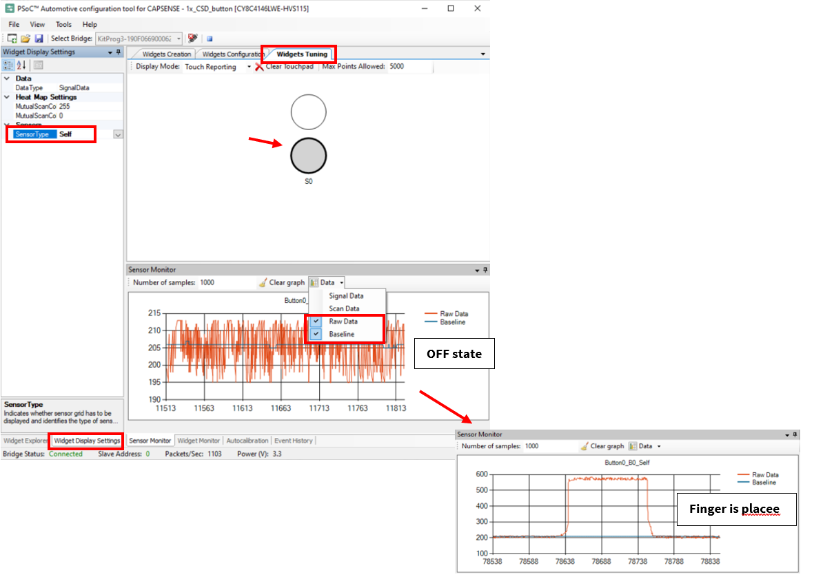
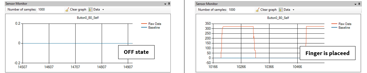
Open PSoCAutomotiveConfigurationTool GUI tool, select the Widgets Display
Settings tab (bottom side), change/confirm Sensor Type =
Self, click S0 (gray color), select the
Raw Data and Baseline. You can
observe the raw data waveform in Sensor Monitor window.Figure 34. Sensor Monitor window
The following values are used in this example:
Average level of raw data in the OFF state = 206
Minimum value of raw data in the OFF state = 195
Maximum value of raw data in the OFF state = 213
Average level of raw data when the finger is placed = 580
Calculate the SNR value:
Signal data = 580 - 206 = 374
OFF noise = 213 – 195 = 18
SNR = 374 / 18 = 20.77
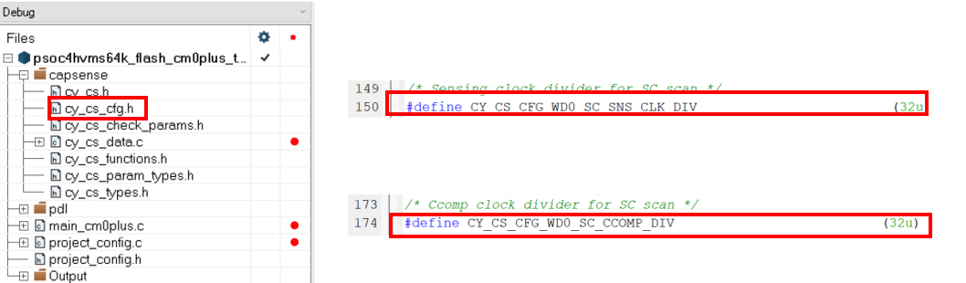
In the IAR EARM tool, open the cy_cs_cfg.h file on
IAR EARM, and update the two sense clock divider parameters to the calculated value
of the sense clock divider (See Table 6).
CY_CS_CFG_WD0_SC_SNS_CLK_DIV
CY_CS_CFG_WD0_SC_CCOMP_DIV
Figure 35. Sense clock divider parameteres
Download the application on IAR EARM.
Open PSoCAutomotiveConfigurationTool GUI tool, click run button and confirm the raw
data waveform.Figure 36. Raw data waveform
Average level of raw data in the OFF state = 0
Minimum value of raw data in the OFF state = 0
Maximum value of raw data in the OFF state = 0
Average level of raw data when the finger is placed = 325
Signal data = 325 - 0 = 325
OFF noise = 0
SNR = ∞
Set number of sub-conversions and scan time
The number of sub-conversions decides the sensitivity of the sensor and sensor scan time.
Increasing the number of sub-conversions (NSub) increases the signal and SNR.
However, increasing the number of sub-conversions also increases the scan time of the
sensor per the following equation.
Figure 37. Number of sub-conversions and scan time
where,
TSCAN = Sensor scan time
NSUB = Number of sub-conversions
FSW = Sense clock frequency
Update the number of sub-conversions (CY_CS_CFG_WD0_SC_SUBCONV_COUNT) on IAR EARM.
Increase or decrease the number of sub-conversions by (e.g. 5) and load the
parameters to the device. The signal level is directly proportional to the number of
sub-conversions.Figure 38. Update the number of sub-conversions on IAR EARM
Note: The sense clock divider and the number of
sub-conversions should be the same for both the sensors scanned in the same
slot. Use the values corresponding to the sensor with the highest
CP.
Measure SNR as mentioned in Section 6.2.3 and tune until the minimum SNR of 10:1
and a raw data count greater than 50 are achieved.
Skip this step if the following conditions are met:
Measured SNR from the previous stage is greater than 10:1.
Raw data count > 50.
If your system is very noisy (e.g. counts < 20), set the scaling factor
(CY_CS_CFG_WD0_SC_SCAL_FACTOR). It can be used to change the number of counts per 1
pF of signal. The default 100% scaling factor provides a signal of approximately 150
counts per pF. Setting this to 200% will provide 300 counts of signal per pF.
Tune threshold parameters
CAPSENSE™ threshold parameters govern
the sensor status based on the raw count of a sensor. Table 7 provides a list of CAPSENSE™ threshold parameters. These parameters apply
to both CSD and CSX sensing methods. This section defines these parameters with the help of
Baseline. Table 7 also shows the
recommended values for the threshold parameters and they are applicable for most of the
designs. However, if there is any external noise present in the end system, you must modify
these thresholds accordingly to avoid any sensor false trigger.
This section explains how to manually tune the mutual-capacitance-based button for optimum performance with respect to parameters such as reliability, power consumption, response time, and linearity using the CSX-RM sensing technique and PSoCAutomotiveConfigurationTool. Here, the crosspoint (CSX) represents the mutual-capacitance between the Tx electrode and Rx electrode and RM represents the ratio-metric method.
Measure the parasitic capacitance (Cp)
Use on-board CSX buttons to measure the Cp value. Both CYHVMS-64K-56-001 and KIT_PSOC4-HVMS-64K_LITE boards can support the CSX buttons.
Take a back-up of the cy_cs_cfg.h file of
the tuned CSD setting if necessary.
Open CSX_buttons.csproject on
PSoCAutomotiveConfigurationTool.exe.
Click Save Project button to generate the
cy_cs_cfg.h file in same folder as the
xxx.csproject path.
Download the application on IAR EARM.
Estimate the Cp of the sensor electrode using the Cy_Cs_GetCpValue() function in
firmware. The measured capacitance value is in femtofarad (fF).
See 6.2.1 for how to
measure the Cp value using the Cy_Cs_GetCpValue() function.
Figure 39. Measure capacitance value
Calculate the Tx clock frequency
The Tx clock frequency determines the duration of each sub-conversion. The Tx clock signal must completely charge and discharge the sensor parasitic capacitance.
Calculate maximum Tx clock frequencies using the following equation.Figure 40. Tx clock frequency
where,
CpTx = Tx electrode parasitic
capacitance. This value is obtained from 6.3.1.
RSeriesTx = Total series-resistance, including the
Rinternal resistance of the internal switches, the
recommended external series resistance of 560 Ω (connected on PCB trace,
connecting sensor pad to the device pin), and trace resistance if using
highly resistive materials (example ITO or conductive ink).
Rinternal = Internal resistance,
this varies based on scan modes, see Table 8.
Table 8. Internal resistance for sensor
Scan mode
Rinternal
CTRLMUX
950 Ω
AMUXBUS
500 Ω
The Tx clock divider value, as given by the following equation, is
obtained by dividing HFCLK (FMOD: e.g., 48 MHz) by Maximum Tx clock
frequency (kHz): FTX calculated and choosing the nearest ceiling Tx clock
divider option in the configurator.Figure 41. Tx clock divider value
Table 9. Tx clock frequency settings for CYHVMS-64K-56-001 from
Cp
Note: The actual sense clock divider value is chosen such that
the divider is divisible by 4, to have all the four scan phases for equal
durations.
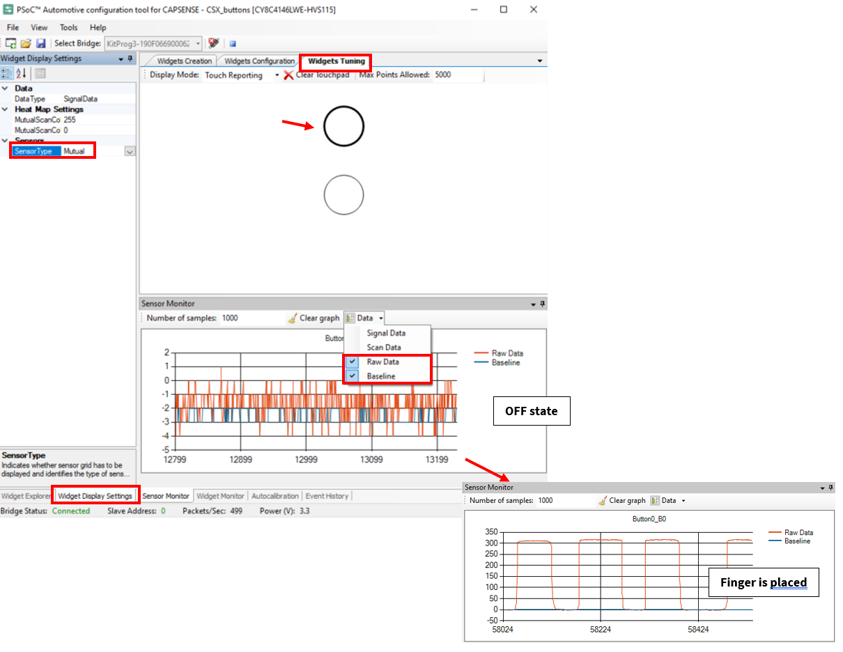
SNR measurement using PSoCAutomotiveConfigurationTool
Open PSoCAutomotiveConfigurationTool, select Widgets Display
Settings tab (bottom side), change/confirm Sensor Type =
Mutual, click B0 button, select the
Raw Data and Baseline. You can
observe the raw data waveform in the Sensor Monitor window.Figure 42. Sensor Monitor window preview
The following values are used in this example:
Average level of raw data in the OFF state = -2
Minimum value of raw data in the OFF state = -4
Maximum value of raw data in the OFF state = 1
Average level of raw data when the finger is placed = 310
Calculate the SNR value:
Signal data = 310 – (-2) = 312
OFF noise = 1 – (-4) = 5
SNR = 312 / 5 = 62.4
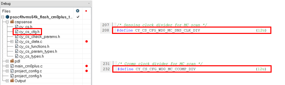
Open the IAR EARM tool, open cy_cs_cfg.h file on IAR
EARM and update the two sense clock divider parameters.
CY_CS_CFG_WD0_MC_SNS_CLK_DIV
CY_CS_CFG_WD0_MC_CCOMP_DIV
Figure 43. Update the two sense clock divider parameters in the IAR EARM
tool
Download the application on IAR EARM.
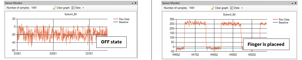
Open the PSoCAutomotiveConfigurationTool tool, rerun and confirm the raw data
waveform.Figure 44. PSoCAutomotiveConfigurationTool tool
Average level of raw data in the OFF state = -20
Minimum value of raw data in the OFF state = -50
Maximum value of raw data in the OFF state = 5
Average level of raw data when the finger is placed = 250
Signal data = 250 – (-20) = 270
OFF noise = 5 – (-50) = 55
SNR = 270 / 55 = 4.90
Note: In the case of this example, the SNR of 10:1 condition is not satisfied due to two CSX buttons used. It needs to increase the value of Tx clock divider (e.g. Tx clock divider uses 24 or more, double of 12) to satisfy the condition.
Set number of sub-conversions and scan time
The number of sub-conversions decides the sensitivity of the sensor and sensor scan time.
Increasing the number of sub-conversions (NSub) increases the signal and SNR.
However, increasing the number of sub-conversions also increases the scan time of the
sensor per the following equation.
Figure 45. Setting number of sub-conversions and scan time
Update the number of sub-conversions (CY_CS_CFG_WD0_MC_SUBCONV_COUNT) on IAR EARM.
Increase or decrease the number of sub-conversions by (e.g. 5) and load the
parameters to the device. The signal level is directly proportional to the number of
sub-conversions.Figure 46. Update the number of sub-conversions on IAR EARM
Note: The Tx clock divider and the number of
sub-conversions should be the same for both the sensors scanned in the same
slot. Use the values corresponding to the sensor with the highest
CP.
Measure SNR as mentioned in Section 6.3.3 and tune until the minimum SNR of 10:1
and a raw data count greater than 50 are achieved.
Skip this step if the following conditions are met:
Measured SNR from the previous stage is greater than 10:1.
Raw data count > 50.
If your system is very noisy (e.g. counts < 20), set Scaling factor
(CY_CS_CFG_WDx_MC_SCAL_FACTOR). It can be used to change the number of counts
per 1 pF of signal. The default 100% scaling factor provide a signal of
approximately 150 counts per pF. Setting this 200% will provide 300 counts of
signal per pF.
Tune threshold parameters
The tuning of threshold parameters is the same value as CSD button tuning.
See 6.2.5 for more details.
Touchpad tuning
This section explains how to manually tune the mutual-capacitance-based touchpad for optimum performance with respect to parameters such as reliability, power consumption, response time, and linearity using the CSX-RM sensing technique and PSoCAutomotiveConfigurationTool.
Measure the parasitic capacitance
(Cp)
Connect Trackpad extension board to
CYHVMS-64K-56-001 evaluation board. Note that KIT_PSOC4-HVMS-64K_LITE is not included in
the extension board.
Take a back-up of the cy_cs_cfg.h file of
tuned CSD or CSX setting if necessary.
Open 9x8_touchpad.csproject on
PSoCAutomotiveConfigurationTool.exe.
Click Save Project button to generate
cy_cs_cfg.h file in same folder as
xxx.csproject path.
Download the application on IAR EARM.
Estimate the CP of the sensor electrode using the
Cy_Cs_GetCpValue() function in firmware. The measured capacitance value is in
femtofarad (fF).
See 6.2.1 for how to
measure the CP value using the Cy_Cs_GetCpValue()
function.
Figure 47. Estimating the CP of the sensor electrode in
firmware
Calculate the Tx clock frequency
The Tx clock frequency is the same equation as CSX button tuning. See 6.3.2 for more details.
Table 10. Tx clock frequency settings for CYHVMS-64K-56-001 from CP
Note: In this example, 8x-TX and 9x-Rx pins are used. Therefore, the Tx clock divider uses
108 (9 × 12).
SNR measurement using PSoCAutomotiveConfigurationTool
Open the PSoCAutomotiveConfigurationTool GUI tool, select Widgets Display
Settings tab (bottom side), change/confirm Sensor Type =
Mutual, change the Display Mode to Heat map.
You can observe the signal data value on each sensor element of the touchpad.Figure 48. Change Display Mode to Heat map
Capture and note the highest/lowest noise of the sensor element (peak-to-peak
noise), without placing a finger (recommend observing the noise value for 3–5
seconds).
In this example:
Minimum value of signal data in the OFF state = –4
Maximum value of signal data in the OFF state = 5
Maximum peak-to-peak noise = 5 – (–4) = 9
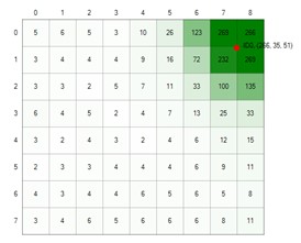
Firmly hold the finger on the touchpad in the least touch intensity
(LTI) position (at the intersection of four nodes) as shown in the following figure.
See AN85951 for more details on the LTI
position.
Note:
Finger movement during the test can artificially increase the noise
level.
The LTI signal is measured at the farthest point of the trackpad from
the sensor pin connection, where the sensors have the worst-case RC-time
constant.
Figure 49. Touchpad preview
Calculate the LTI Signal:
LTI Signal = (269 + 266 + 232 + 269) / 4 = 259
Calculate the SNR value using the following equation:Figure 50. SNR value
SNR = 259 / 9 = 28.77
Open the IAR EARM tool, open cy_cs_cfg.h file on IAR EARM,
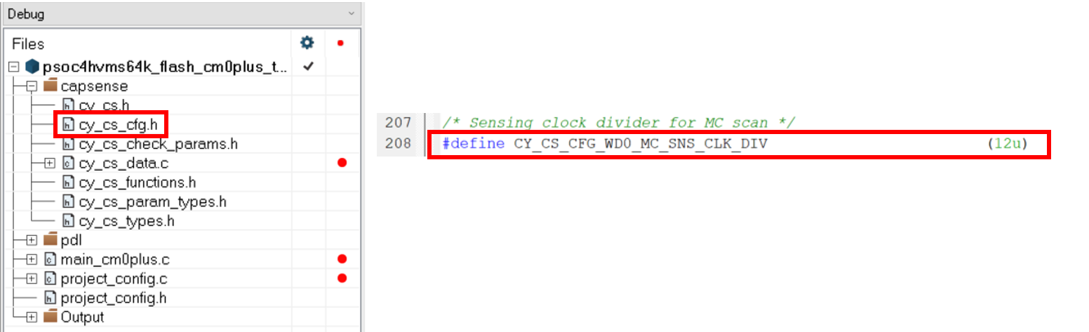
and update two Tx clock divider parameters (See Table 10).
CY_CS_CFG_WD0_MC_SNS_CLK_DIV
CY_CS_CFG_WD0_MC_CCOMP_DIV
Figure 51. Updating Tx clock divider parameters
Download the application on IAR EARM.
Open PSoCAutomotiveConfigurationTool GUI tool, rerun and confirm the SNR.
Minimum value of signal data in the OFF state = -2
Maximum value of signal data in the OFF state = 4
Maximum peak-to-peak noise = 4 – (-2) = 6
LTI Signal = (260 + 258 + 225 + 263)/4 = 251.5
SNR = 251.5/6 = 41.91
Set number of sub-conversions and scan time
The sub-conversions and scan time settings are the same equation as CSX
button tuning. See 6.3.4.
Tune threshold parameters
The tuning of threshold parameters is the same value as CSD button tuning.
See 6.2.5.
Summary
This application note has described details of the CAPSENSE™ (multi-sense converter) block of PSOC™ HV MS MCU. By
using the CAPSENSE™ (multi-sense converter) block, human machine
interface (HMI), body, and power-train applications can be achieved with higher quality.
Infineon provides an evaluation board and a wealth of sample software to help you get
started with PSOC™ HV MS family MCUs. To evaluate the evaluation board,
contact your sales representative or Infineon Technical Support.
Glossary
Table 11. Glossary
Terms
Description
3W
3 width
ADC
analog to digital converter
AMD
Advanced Micro Devices, Inc. (company name)
AMUX
analog multiplexer
API
application programming interface
AutoPDL
automotive peripheral driver library
Arm®
Advanced RISC Machine (company name)
ASIL-B
automotive safety integrity level - B
ASPICE
automotive software process improvement and capability determination
BIST
built in self-test
CAPDAC
capacitor digital to analog converter
CAPSENSE™
capacitive sensing
CDAC
capacitor digital to analog converter
CERT
computer emergency response team
CM0+
Arm®
Cortex®-M0+ (processor core name)
CLK
clock
CMOD
modulator capacitor
CMRR
common mode rejection ratio
CP
parasitic capacitance
CPU
central processing unit
CSB
CAPSENSE™ button
CST
CAPSENSE™ touchpad
CSD
CAPSENSE™ sigma delta
(self-capacitance)
CSX
CAPSENSE™ crosspoint
(mutual-capacitance)
CTRL
control
CTRLMUX
control multiplexer
DMA
direct memory access
ENIG
electroless nickel/immersion gold
fF
femtofarad
FW
firmware
GND
ground
GPIO
general purpose I/O
GUI
graphical user interface
HFCLK
high frequency clock
HMI
human machine interface
HV
high-voltage
HW
hardware
I/O
input or output
IAR
IAR Systems (company name)
IAR EARM
IAR Embedded Workbench for Arm®
(software name)
IC
integrated circuit
IDAC
current digital to analog converter
ISO
international organization for standardization
ITO
indium tin oxide
LED
light emitting diode
LIN
local interconnect network
LTI
least touch intensity
MUX
multiplexer
MW
middleware
MSC
multi-sense converter
MCU
microcontroller unit
MISRA
motor industry software reliability association
MS
mixed signal
PCB
printed circuit board
PELI
peripheral
pF
picofarad
PHY
physical layer
PSOC™
programmable system on chip
PWM
pulse width modulation
QFN
quad flat non-leaded
RF
radio frequency
RM
ratiometric method
RX
receiver
SAR
successive approximation register
SEooC
safety element out of context
SNR
signal-to-noise ratio
SW
switch
TX
transmitter
References
The following documents are PSOC™ HV MS family series application notes,
datasheets, and reference manuals. Contact Technical
Support to obtain these documents and a sample driver library.