AN233648 PSoC™ 6 MCU: Modify CY8CPROTO-062-4343W board to work with an external flash memory

About this document
Scope and purpose
This application note describes steps to enable a CY8CPROTO-062-4343W PSoC™ 6 Wi-Fi Bluetooth® prototyping kit to work with an external flash memory by modifying the board hardware and software. By replacing the attached flash with the external connection and adding commands into PSoC™ 6 MCU serial memory interface (SMIF), this board can be turned into a memory evaluation board for any external flash.
Intended audience
This application note targets PSoC™ 6 MCU board users who intend to further investigate operation with external flash memory devices other than the offered S25FL512S flash on the board. This method will free the limitation of the users to evaluate any flash. The flash device in the SOIC-16 package on the board may be replaced freely; the external flash outside the board with any type of package can be tested.
Introduction
Figure 1. CY8CPROTO-062-4343W PSoC™ 6 Wi-Fi Bluetooth® prototyping board
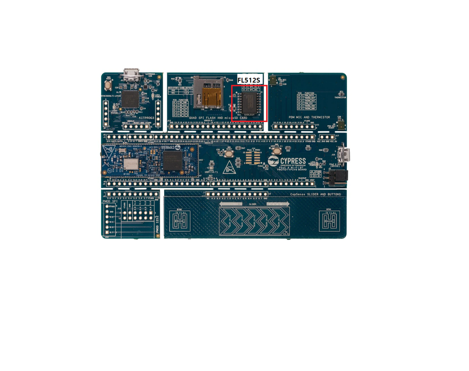
The PSoC™ 6 Wi-Fi Bluetooth® prototyping kit (CY8CPROTO-062-4343W) is provided with the S25FL512S 512-Mb SPI NOR flash using SMIF. SMIF is an SPI-based communication interface for interfacing external devices to a PSoC™ MCU device. However, as this PSoC™ 6 MCU board comes with external flash attached to the board. Because there are several commands to evaluate all flash operations, there are limitations on evaluating flash memories fully. This application note describes a method to modify this PSoC™ 6 MCU board hardware and software for customizing the board into a general evaluation tool for flash memory devices.
Procedures
Both hardware and software modifications are required for this application.
Modifying the hardware
Materials required
Figure 2. SMT socket – wide SOIC-16, pin header
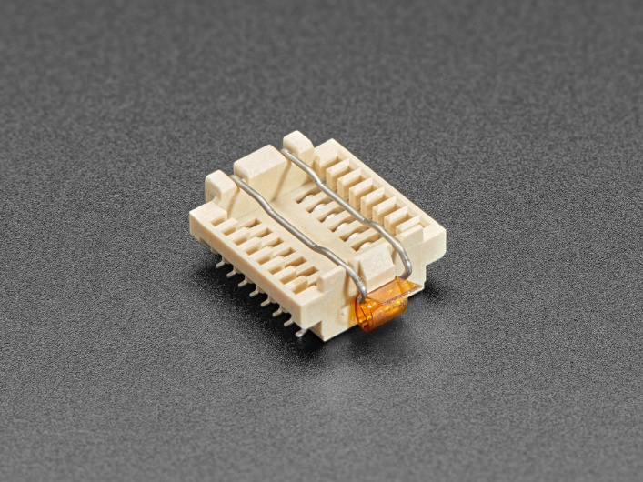
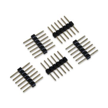
- CY8CPROTO-062-4343W PSoC™ 6 W-Fi Bluetooth® prototyping kit board
- SMT socket-wide SOIC-16
- 8-pin headers
- Cutter
- Soldering machine
Customize the board
Prepare the board and SMT socket-wide SOIC-16, and 8-pin headers. You may also need a cutter to remove the existing flash device and a soldering machine to solder the socket and pin headers.
- Remove the attached flash with the cutter. Gently cut off the flash lead frames and then remove the leftovers with solders. Be careful not to strip off the PCB pattern
- Fit the SMT socket-wide SOIC-16 into the PCB footprint. The existing flash on the board is in SOIC 16 pin package, so it is compatible with the new socket. Solder the socket along the footprint
- Solder the pin headers to GND, VDDIO, pins 11.6, 11.5, 11.7, 11.2, 11.3, and 11.4 pin holes. See Table 1 and Figure 3
- Make sure that all pins are connected
| Pin | Flash | Pin | Flash |
|---|---|---|---|
GND | VSS | P11.7 | SCK |
VDDIO_O | VCC | P11.2 | #CS |
P11.6 | SI/IO0 | P11.3 | HOLD/IO3 |
P11.5 | SO/IO1 | P11.4 | WP/IO2 |
Figure 3. Board pinout
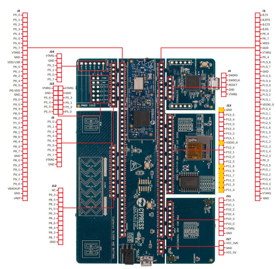
Test the flash devices as follows:
- To test any flash device in SOIC-16 package, replace the flash chip in the socket as shown in Figure 5
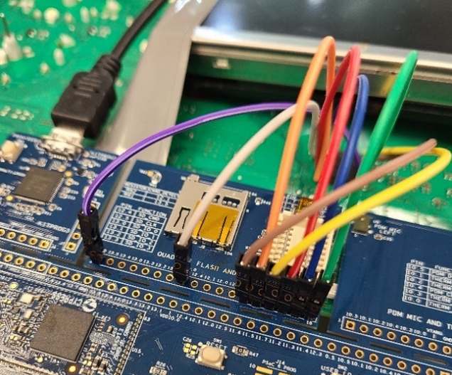
- To test flash devices in other package types or to test the flash device that is attached to another board like shown in Figure 6, use the pin header connector. In this case, keep the socket empty because the socket flash signal and external signal through pin header can be overlapped
Figure 4. CY8CPROTO-062-4343W external connections
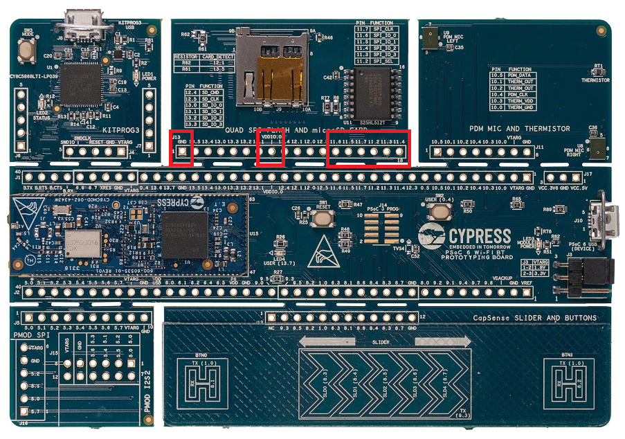
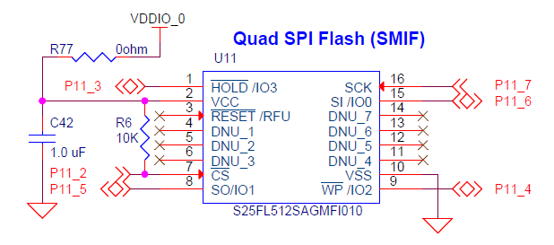
Figure 5 and Figure 6 show the boards with the hardware modifications:
- Figure 5 shows the flash device in the socket being tested
- Figure 6 shows an external flash device on another board being tested. Note that the jumpers are connected to the pin header while the socket is empty
Figure 5. PSoC™ 6 MCU board with the socket attached
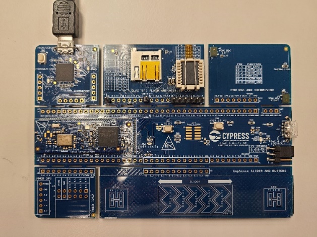
Figure 6. External flash memory connected with a pin header
Modifying the software
ModusToolbox™ software
PSoC™ 6 MCU boards use Eclipse IDE for ModusToolbox™ and C language for programming.

Download the software from https://www.cypress.com/products/modustoolbox#tabs-0-bottom_side-6.
Serial memory interface (SMIF)
The SMIF Component implements an SPI-based communication hardware block for interfacing external memory devices with the PSoC™ 6 MCU device. The firmware uses the source code (cy_smif_memconfig.c and cy_smif_memconfig.h files) generated from the SMIF configurator. This source code defines the data structures that hold the memory configuration.
Import ModusToolbox QSPI flash code example
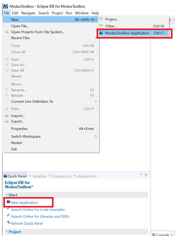
On Eclipse IDE for ModusToolbox™ software, import example project into your project. Do one of the following:
Select
Click New Application on the Start tab on the Quick Panel
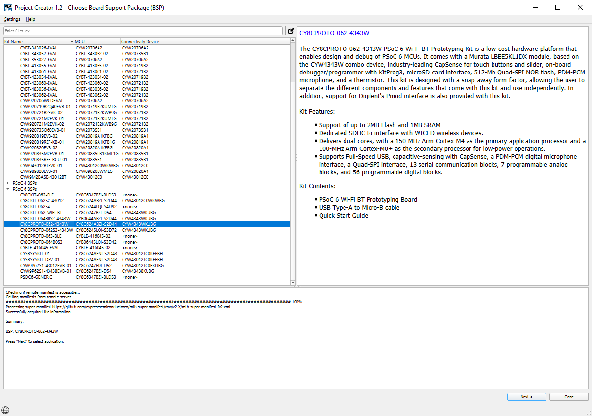
Choose the board support package (BSP) for the CY8CPROTO-062-4343W board and then click Next
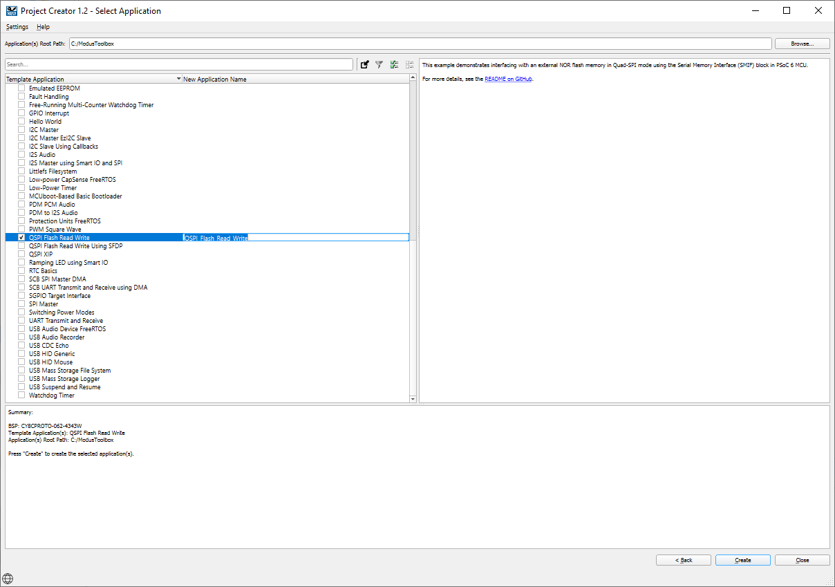
On the Select Application window, select QSPI Flash Read Write. Optionally, change the application name
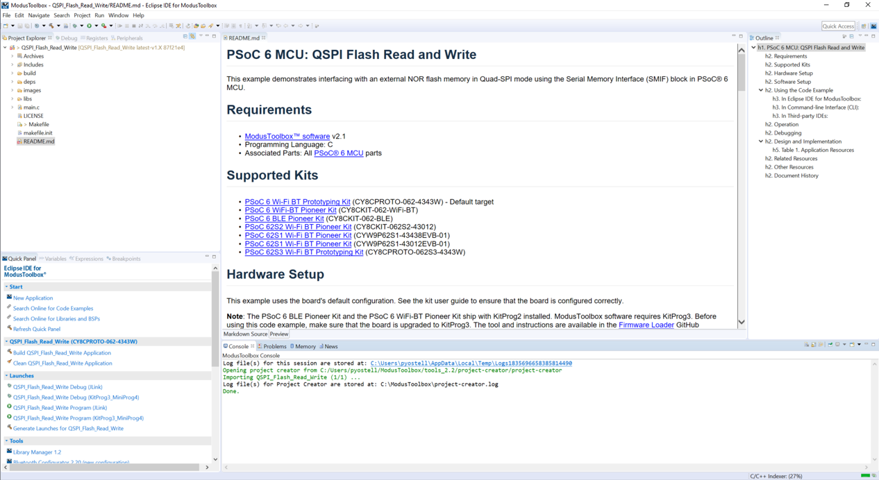
The following screen appears when the selected example is successfully imported:
Determine the serial flash operation structure
Note that the application already includes supports for some flash operation commands for QSPI Flash Read and Write operation. The cy_smif_memslot.h file includes code to support the WRR(01h), WRDI(04h), RDSR1(05h), WREN(06h), 4QPP(34h), RDCR(35h), BE(60h), 4SE(DCh), and 4QIOR(ECh) commands. However, these commands may not be sufficient to test all flash operations.
Code Listing 1: Built-in functions in cycfh_qspi_memslot.c
typedef struct
{
/*This specifies the number of address bytes used by the memory slave device, valid values 1-4 */
  uint32_t numOfAddrBytes;
  /*The memory size: For densities of 2 gigabits or less - the size in bytes; For densities 4 gigabits and above - bit-31 is set to 1b to define that this memory is 4 gigabits and above; and other 30:0 bits define N where the density is computed as 2^N bytes. For example, 0x80000021 corresponds to 2^30 = 1 gigabyte.*/
  uint32_t memSize;
/*This specifies the Read command */
  cy_stc_smif_mem_cmd_t* readCmd;
/*This specifies the Write Enable command */
  cy_stc_smif_mem_cmd_t* writeEnCmd;
/*This specifies the Write Disable command */
  cy_stc_smif_mem_cmd_t* writeDisCmd;
/*This specifies the Erase command */
  cy_stc_smif_mem_cmd_t* eraseCmd;
/*This specifies the sector size of each Erase */
  uint32_t eraseSize;
/*This specifies the Chip Erase command */
  cy_stc_smif_mem_cmd_t* chipEraseCmd;
/*This specifies the Program command */
  cy_stc_smif_mem_cmd_t* programCmd;
/*This specifies the page size for programming */
  uint32_t programSize;
/*This specifies the command to read the WIP-containing status register */
  cy_stc_smif_mem_cmd_t* readStsRegWipCmd;
/*This specifies the command to read the QE-containing status register */
  cy_stc_smif_mem_cmd_t* readStsRegQeCmd;
/*This specifies the command to write into the QE-containing status register */
  cy_stc_smif_mem_cmd_t* writeStsRegQeCmd;
/*This specifies the read SFDP command */
  cy_stc_smif_mem_cmd_t* readSfdpCmd;
/*This specifies the Read ID command */
  cy_stc_smif_mem_cmd_t* readIDCmd;
/* The Busy mask for the status registers */
  uint32_t stsRegBusyMask;
/*The QE mask for the status registers */
  uint32_t stsRegQuadEnableMask;
/*Max time for erase type 1 cycle time in ms*/
  uint32_t eraseTime;
/*Max time for chip erase cycle time in ms */
  uint32_t chipEraseTime;
/*Max time for page program cycle time in us */
  uint32_t programTime;
/*This specifies the number of regions for memory with hybrid sectors */
  uint32_t hybridRegionCount;
/*This specifies data for memory with hybrid sectors */
  cy_stc_smif_hybrid_region_info_t** hybridRegionInfo;
} cy_stc_smif_mem_device_cfg_t;
This section provides steps to add additional operation commands other than the commands provided by the example code. The flash commands vary from the products and the interface—see the datasheet for each flash for supported command sets.
For example, a brief list of supported commands for the S25FL512S device is in shown in Table 2. See the datasheet for detailed descriptions for each command.
The example code provided commands WRR(01h), WRDI(04h), RDSR1(05h), WREN(06h), 4QPP(34h), RDCR(35h), BE(60h), 4SE(DCh), 4QIOR(ECh) are shown in Bold.
| Instruction (in HEX) | Command name | Instruction (in HEX) | Command name |
|---|---|---|---|
| 01 | WRR | 6C | 4QOR |
| 02 | PP | 75 | ERSP |
| 03 | READ | 7A | ERRS |
| 04 | WRDI | 85 | PGSP |
| 05 | RDSR1 | 8A | PGRS |
| 06 | WREN | 90 | READ_ID |
| 07 | RDSR2 | 9F | RDID |
| 0B | FAST_READ | A3 | MPM |
| 0C | 4FAST_READ | A6 | PLBWR |
| 0D | DDRFR | A7 | PLBRD |
| 0E | 4DDRFR | AB | RES |
| 12 | 4PP | B9 | BRAC |
| 13 | 4READ | BB | DIOR |
| 14 | ABRD | BC | 4DIOR |
15 | ABWR | BD | DDRDIOR |
16 | BRRD | BE | 4DDRDIOR |
17 | BRWR | C7 | BE |
18 | ECCRD | D8 | SE |
20 | P4E | DC | 4SE |
21 | 4P4E | E0 | DYBRD |
2B | ASPRD | E1 | DYBWR |
2F | ASPP | E2 | PPBRD |
30 | CLSR | E3 | PPBP |
32 | QPP | E4 | PPBE |
34 | 4QPP | E5 | Reserved-E5 |
35 | RDCR | E6 | Reserved-E6 |
38 | QPP | E7 | PASSRD |
3B | DOR | E8 | PASSP |
3C | 4DOR | E9 | PASSU |
41 | DLPRD | EB | QIOR |
42 | OTPP | EC | 4QIOR |
43 | PNVDLR | ED | DDRQIOR |
4A | WVDLR | EE | 4DDRQIOR |
4B | OTPR | F0 | RESET |
60 | BE | FF | MBR |
6B | QOR |
Use the top-down approach on the codes to determine the architecture of the serial flash memory operation.
For example, consider the cy_serial_flash_qspi_read operation starting from main.c to investigate the SMIF structure.
Figure 7. SMIF structure
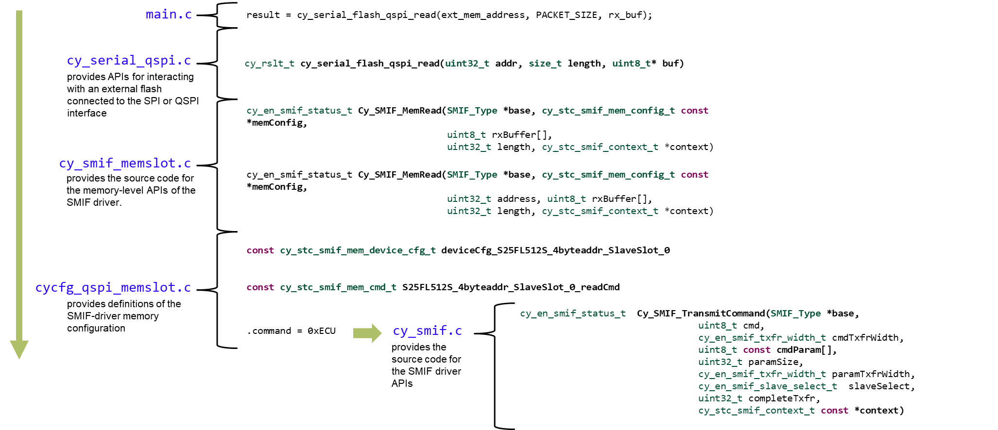
By exploring from main.c and all the way down to cy_smif.c, you can determine that the actual operation command is delivered to Cy_SMIF_TransmitCommand in cy_smif.c with command arguments, command width, address width, mode, mode width, the number of dummy cycles, and data width. The arguments are specified in cycfg_qspi_memslot.c for each operation command.
Code Listing 2: S25FL512S_4byteaddr_SlaveSlot_0_readCmd in
cycfg_qspi_memslot.c
const cy_stc_smif_mem_cmd_t
   S25FL512S_4byteaddr_SlaveSlot_0_readCmd =
     {
       /* The 8-bit command. 1 x I/O read command. */
       .command = 0xECU,
       /* The width of the command transfer. */
       .cmdWidth = CY_SMIF_WIDTH_SINGLE,
       /* The width of the address transfer. */
       .addrWidth = CY_SMIF_WIDTH_QUAD,
       /* The 8-bit mode byte. This value is 0xFFFFFFFF when there is no mode present. */
       .mode = 0x01U,
       /* The width of the mode command transfer. */
       .modeWidth = CY_SMIF_WIDTH_QUAD,
       /* The number of dummy cycles. A zero value suggests no dummy cycles. */
       .dummyCycles = 4U,
       /* The width of the data transfer. */
       .dataWidth = CY_SMIF_WIDTH_QUAD
     };
See the datasheet for the argument values in the command sequence.
Figure 8. Quad I/O Read command sequence (4-byte address, ECh or EBh)

Add additional flash operation commands
To add an additional command other than the supported commands, reverse the top-down approach. This is demonstrated with the RDID (9Fh) command.
Check the command sequence for RDID 9Fh
Figure 9. Read Identification (RDID 9Fh) command sequence

Specify the arguments for the operation command in
cycfg_qspi_memslot.cto define theSMIF-drivermemory configurationCode Listing 3: S25FL512S_4byteaddr_SlaveSlot_0_readIDCmd in cycfg_qspi_memslot.c
const cy_stc_smif_mem_cmd_t
S25FL512S_4byteaddr_SlaveSlot_0_readIDCmd =
{
  /* The 8-bit command. 1 x I/O read command. */
  .command = 0x9FU,
  /* The width of the command transfer. */
  .cmdWidth = CY_SMIF_WIDTH_SINGLE,
  /* The width of the address transfer. */
  .addrWidth = CY_SMIF_WIDTH_NA,
  /* The 8-bit mode byte. This value is 0xFFFFFFFF when there is no mode present. */
  .mode = 0xFFFFFFFFU,
  /* The width of the mode command transfer. */
  .modeWidth = CY_SMIF_WIDTH_NA,
  /* The number of dummy cycles. A zero value suggests no dummy cycles. */
  .dummyCycles = 0U,
  /* The width of the data transfer. */
  .dataWidth = CY_SMIF_WIDTH_SINGLE
};
Add the read ID command to the command structure in cycfg_qspi_memslot.c
Code Listing 4: deviceCfg_S25FL512S_4byteaddr_SlaveSlot_0 in cycfg_qspi_memslot.c
const cy_stc_smif_mem_device_cfg_t
deviceCfg_S25FL512S_4byteaddr_SlaveSlot_0 =
  {
    ...
    .readIDCmd =
(cy_stc_smif_mem_cmd_t*)&S25FL512S_4byteaddr_SlaveSlot_0_readIDCmd,
    ...
  }
Add the function that actually operates the command in
cy_smif_memslot.cwhere the source code for memory-level APIs for the SMIF driver is providedCode Listing 5: Cy_SMIF_MemCmdReadID in cy_smif_memslot.c
cy_en_smif_status_t Cy_SMIF_MemCmdReadID(SMIF_Type *base,
                             cy_stc_smif_mem_config_t const *memDevice,
                             uint8_t* readBuff,
                             uint32_t size,
                             cy_stc_smif_context_t *context)
{
  cy_en_smif_status_t result = CY_SMIF_BAD_PARAM;
  cy_en_smif_slave_select_t slaveSelected;
  cy_stc_smif_mem_device_cfg_t *device = memDevice->deviceCfg;
  cy_stc_smif_mem_cmd_t *cmdReadID = device->readIDCmd;
  if(NULL == cmdReadID)
  {
    result = CY_SMIF_CMD_NOT_FOUND;
  }
  else
  {
    slaveSelected = (0U == memDevice->dualQuadSlots)?memDevice->slaveSelect:
                    (cy_en_smif_slave_select_t)memDevice->dualQuadSlots;
    result = Cy_SMIF_TransmitCommand( base,
             (uint8_t)cmdReadID->command,
             cmdReadID->cmdWidth,
             CY_SMIF_CMD_WITHOUT_PARAM, CY_SMIF_CMD_WITHOUT_PARAM,
                     CY_SMIF_WIDTH_NA,
             slaveSelected, CY_SMIF_TX_NOT_LAST_BYTE, context);
    if(CY_SMIF_SUCCESS == result)
    {
      result = Cy_SMIF_ReceiveData(base, readBuff, size,
                     cmdReadID->dataWidth, NULL, context);
    }
  }
  return(result);
}
Add the function that returns the data to the
rxBuffer in cy_smif_memslot.cwhere the source code for memory-level APIs for the SMIF driver is providedCode Listing 6: Cy_SMIF_MemCmdReadID in cy_smif_memslot.c
cy_en_smif_status_t Cy_SMIF_MemReadID(SMIF_Type *base,
                cy_stc_smif_mem_config_t const *memConfig,
                uint8_t rxBuffer[],
                uint32_t length,
                cy_stc_smif_context_t *context)
{
  cy_en_smif_status_t status = CY_SMIF_BAD_PARAM;
  uint32_t chunk = 0UL;
  CY_ASSERT_L1(NULL != memConfig);
  CY_ASSERT_L1(NULL != rxBuffer);
  if(1)
  {
       /* SMIF can read only up to 65536 bytes in one go. Split the larger
          read into multiple chunks */
    while (length > 0UL)
    {
       /* Get the number of bytes which can be read during one operation */
      chunk = (length > SMIF_MAX_RX_COUNT) ?
                  (SMIF_MAX_RX_COUNT) : length;
       /* Send the command to read data from the external memory to the rxBuffer array */
       status = Cy_SMIF_MemCmdReadID(base, memConfig,
                  (uint8_t *)rxBuffer, chunk, context);
       if(CY_SMIF_SUCCESS == status)
         {
            /* Wait until the SMIF block completes receiving data */
            status = PollTransferStatus(base, CY_SMIF_REC_CMPLT, context);
         }
         if(CY_SMIF_SUCCESS != status)
         {
           break;
         }
         /* Recalculate the next rxBuffer offset */
         length -= chunk;
         rxBuffer = (uint8_t *)rxBuffer + chunk;
    }
  }
  return status;
}
Add the function that executes the read ID operation to the external flash in
cy_serial_flash_qspi.cwhere it provides APIs for interacting with an external flashCode Listing 7: cy_serial_flash_qspi_readID in cy_serial_flash_qspi.c
cy_rslt_t cy_serial_flash_qspi_readID(size_t length,
                              uint8_t* buf)
{
  cy_rslt_t result_mutex_rel = CY_RSLT_SUCCESS;
  cy_rslt_t result = _mutex_acquire();
  if (CY_RSLT_SUCCESS == result)
  {
    /* Cy_SMIF_MemReadID() returns error if (addr + length) > total flash
            size.*/
    result = (cy_rslt_t)Cy_SMIF_MemReadID(qspi_obj.base,
                qspi_block_config.memConfig[MEM_SLOT],
                buf, length,
                &qspi_obj.context);
                result_mutex_rel = _mutex_release();
    result_mutex_rel = _mutex_release();
  }
  /* Give priority to the status of SMIF operation when both SMIF
            operation and mutex release fail.*/
            return ((CY_RSLT_SUCCESS == result) ? result_mutex_rel :
                         result);
}
In
main.c, add the function to operate the read device RDID (9Fh) operationCode Listing 8: cy_serial_flash_qspi_readID in main.c
int main(void)
{
...
     printf("\r\n1. Reading device ID\r\n");
     result = cy_serial_flash_qspi_readID(DEVICE_ID, rx_buf);
     check_status("Reading Device ID failed", result);
     printf("Byte Address: Data\r\n");
     for(uint8_t i = 0; i < DEVICE_ID; i++)
       printf("0x%02dh : 0x%02Xh \r\n", i, rx_buf[i]);
...
}
Make sure to include the added functions to the header files also.
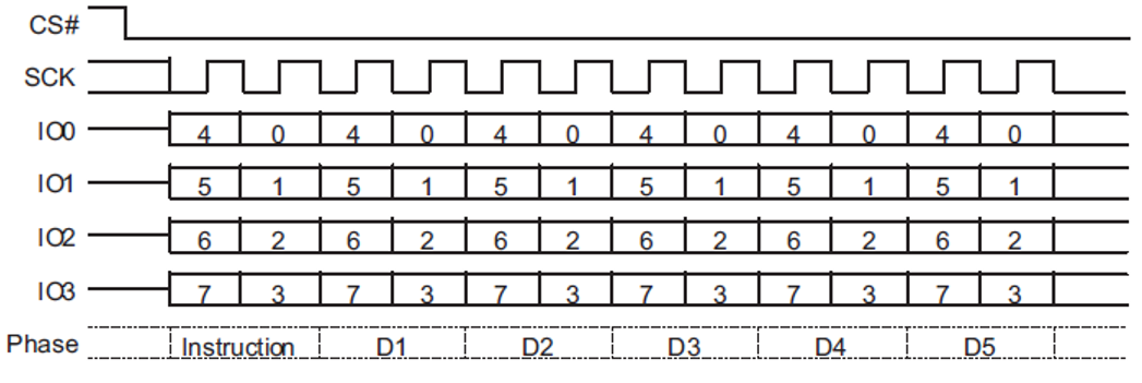
This example code is in SPI mode. Some flash devices such as S25FS512S supports QPI mode, so if you want to operate RDID (9Fh) in QPI mode, you can modify the command width and data width into Quad.
Figure 10. Read Identification (RDID) QPI mode command
Code Listing 9: RDID(9Fh) in QPI mode
const cy_stc_smif_mem_cmd_t
S25FL512S_4byteaddr_SlaveSlot_0_readIDQPICmd =
{
  /* The 8-bit command. 1 x I/O read command. */
  .command = 0x9FU,
  /* The width of the command transfer. */
  .cmdWidth = CY_SMIF_WIDTH_QUAD,
  /* The width of the address transfer. */
  .addrWidth = CY_SMIF_WIDTH_NA,
  /* The 8-bit mode byte. This value is 0xFFFFFFFF when there
             is no mode  present. */
  .mode = 0xFFFFFFFFU,
  /* The width of the mode command transfer. */
  .modeWidth = CY_SMIF_WIDTH_NA,
  /* The number of dummy cycles. A zero value suggests no dummy cycles. */
  .dummyCycles = 0U,
  /* The width of the data transfer. */
  };
PSoC™ 6 MCU board operation
Figure 11 shows the waveforms with the QPI bit set for the FS512S RDID QPI operation signals measured with an oscilloscope. Normally, input signal instructions are latched on the rising edge of the SCK signal. Then, the data output changes after the falling edge of SCK in SDR commands. Because this is a QPI operation, the output data should come after the first 8-bits of the two serial clock instructions on the falling edge. However, for this PSoC™ 6 MCU board, the signals remain HIGH even after the instruction phase; the data phase comes after A certain hold time. This hold time is driven by the controller.
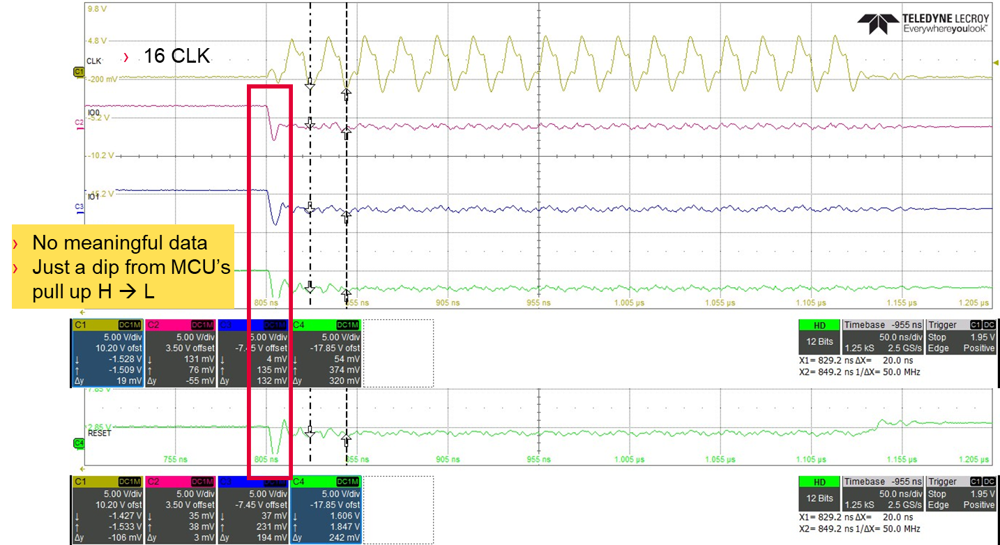
Even though the flash memory is sending data signals after the instruction phase, the controller’s pull-up signal is more dominant, thus ignoring the flash device’s first data signal. Therefore, as soon as the controller drops the bus, a dip can be made regardless of the real signal due to the controller’s sudden drop from HIGH to LOW. Therefore, in the oscilloscope measurements’ point of view, the first data should be read right after the dip but before the second falling edge of the flash device-driven phase. This is because the flash device’s output data is already on the signal bus but ignored due to controller’s control over the bus.
Figure 11. FS512S QPI bit set RDID(9Fh) QPI operation
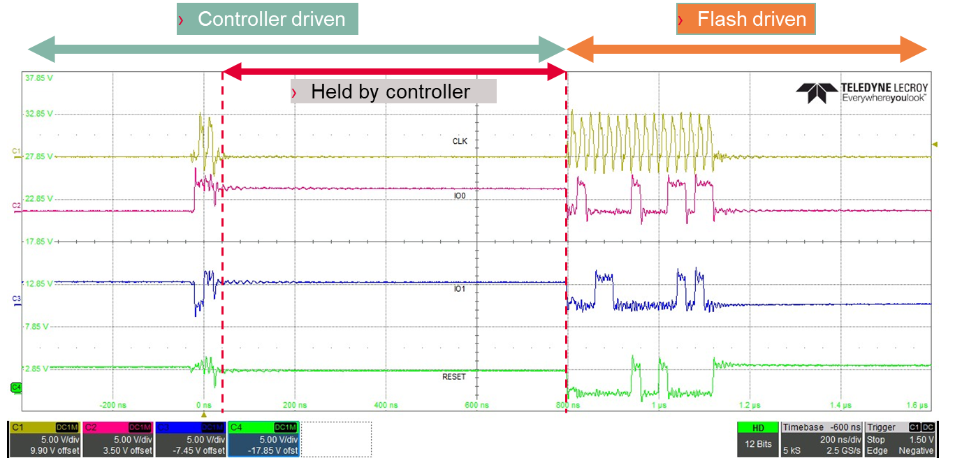
Figure 12. No meaningful dip at the beginning of the data phase
Use cases
Even though these changes make the kit a general flash evaluation tool, its usage can be expanded beyond a demo board. Here’s an actual use case to a customer’s board. When a failure case is submitted, application-level investigation should be done to narrow down the root cause of the failure before failure analysis (FA) is done at the chip level.
Note that the jumpers are connected to the connector pinout on the PCB; it is then connected to the pin header of the PSoC™ 6 MCU board to avoid damage on the target board.
Figure 13. PSoC™ 6 MCU board connected externally to a customer’s application board
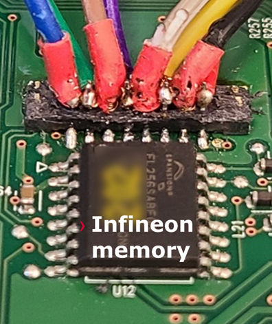
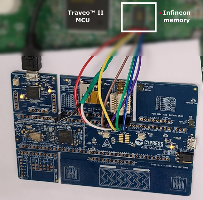
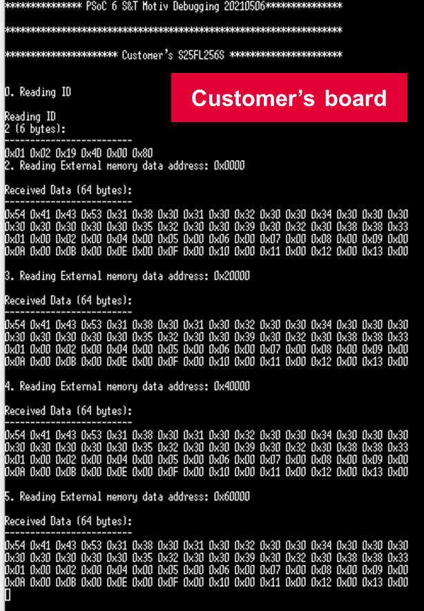
By reading the device ID using the function added and reading the data on a specific address, identical abnormal operation was reproduced with PSoC™ 6 MCU board.
Figure 14. Read ID operation result
Conclusion
Even though CY8CPROTO-062-4343W PSoC™ 6 prototyping kit is provided with a Quad SPI flash device and example code, its use as a general-purpose flash evaluation tool is limited. By modifying the hardware and software of the board, it can be turned into a general tool to operate any flash device.
By attaching a socket, the flash device can be replaced with any SOIC package flash. By attaching pin headers, it frees the spatial constraints and connects any flash device with any package and even to the flash device on an external board. By adding operation commands, the test range can be extended to any commands.
By using the information in this application note, you will be able to make your own PSoC™ 6 MCU-based flash evaluation tool.
References
PSoC™ 6 Wi-Fi Bluetooth® prototyping kit (CY8CPROTO-062-4343W)
CY8CPROTO-062-4343W PSoC™ 6 Wi-Fi Bluetooth® prototyping kit guide
CY8CPROTO-062-4343W schematic
S25FL512S, 512 Mb (64 MB), 3.0 V SPI flash memory datasheet
https://www.cypress.com/documentation/datasheets/s25fl512s-512-mb-64-mb-30-v-spi-flash-memory
ModusToolbox™ software download link
https://www.cypress.com/products/modustoolbox#tabs-0-bottom_side-6
ModusToolbox™ software installation guide
ModusToolbox™ software user guide
Revision history
| Document version | Date of release | Description of changes |
|---|---|---|
** | 2021-09-17 | New application note |
| *A | 2022-07-21 | Template update |