AN210781 Getting started with PSoC™ 6 MCU with Bluetooth® low energy connectivity on PSoC™ Creator
About this document
Scope and purpose
AN210781 introduces you to PSoC™ 6 MCU with Bluetooth® Low Energy connectivity, a dual-CPU Arm® Cortex®-M4 and Cortex®-M0+ based programmable system-on-chip that integrates a Bluetooth® Low Energy 5.0 system, the latest-generation of CAPSENSE™ technology, and a host of security features. This application note helps you explore the PSoC™ 6 MCU with Bluetooth® Low Energy architecture and development tool and shows you how to create your first project using PSoC™ Creator, export the project to a third-party integrated development environment (IDE), and continue your firmware development. It also guides you to more resources available online to accelerate your learning about PSoC™ 6 MCU with Bluetooth® Low Energy connectivity. To get started with the PSoC™ 6 MCU device family, see AN221774 – Getting started with PSoC™ 6 MCU.
To access an ever-growing list of hundreds of PSoC™ code examples, please visit our code examples web page. You can also explore the PSoC™ video library here.
Introduction
PSoC™ 6 MCU with Bluetooth® LE connectivity, hereafter called as PSoC™ 6-BLE, is an ultra-low-power PSoC™ device specifically designed for wearables and Internet of Things (IoT) products. It establishes a new low-power standard for today’s “always-on” applications. The PSoC™ 6 -BLE device is a programmable embedded system-on-chip that integrates the following on a single chip:
- Dual-CPU microcontroller: CM4 and CM0+
- Bluetooth® LE 5.0 subsystem
- Programmable analog and digital peripherals
- Up to 1 MB of flash and 288 KB of SRAM
- Fourth-generation CAPSENSE™ technology
PSoC™ 6-BLE is suitable for a variety of power-sensitive connected applications such as:
- Smart watches and fitness trackers
- Connected medical devices
- Smart home sensors and controllers
- Smart home appliances
- Gaming controllers
- Sports, smart phone, and virtual reality (VR) accessories
- Industrial sensor nodes
- Industrial logic controllers
- Advanced remote controllers
PSoC™ 6-BLE provides a cost-effective and small-footprint alternative to the combination of an MCU and a Bluetooth® LE radio. The programmable analog and digital subsystems allow flexibility and dynamic fine-tuning of the design using PSoC™ Creator the schematic-based design tool for developing PSoC™ 6-BLE applications. To develop a BLE application, you do not need a working knowledge of the complex BLE protocol stack.
PSoC™ 6-BLE is an easy-to-configure, no-cost GUI-based Bluetooth® LE component in PSoC™ Creator that abstracts the protocol complexity.
Bluetooth® LE is an ultra-low-power wireless standard defined by the Bluetooth® Special Interest Group (SIG) for short-range communication. PSoC™ 6-BLE integrates a Bluetooth® LE 4.2 radio and a royalty-free protocol stack with enhanced security, privacy, and throughput compliant with the BLE 5.0 specification.
Fourth-generation capacitive touch-sensing feature in PSoC™ 6-BLE devices, known as CAPSENSE™, offers unprecedented signal-to-noise ratio (SNR); best-in-class waterproofing; and a wide variety of sensor types such as buttons, sliders, track pads, and proximity sensors. CAPSENSE™ user interfaces are gaining popularity in wearable electronic devices such as activity monitors and health and fitness equipment. The CAPSENSE™ solution works in noisy environments and in the presence of liquids.
PSoC™ 6-BLE enables ultra-low-power connected applications with an integrated solution.
Figure 1 shows the application-level block diagram of a fitness tracker based on PSoC™ 6-BLE.
Figure 1. Fitness tracker application block diagram
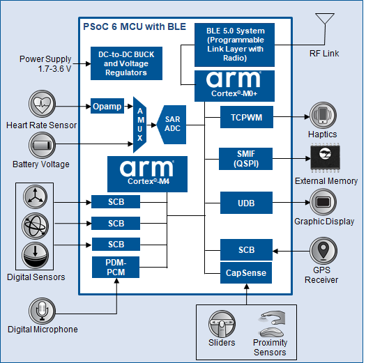
The device provides a one-chip solution and includes:
- A low-power Bluetooth® LE 5.0 system that can sustain up to four simultaneous connections
- A buck converter for ultra-low-power operation
- An analog front end (AFE) within the device to condition and measure heart rate sensor outputs and to monitor battery voltage
- Serial communication blocks (SCBs) to interface with multiple digital sensors including a global positioning system (GPS) module
- A Pulse-Density Modulation (PDM) Pulse Code Modulation (PCM) hardware engine and digital microphone interface for voice
- CAPSENSE™ technology for reliable touch and proximity sensing
- A serial memory interface (SMIF) that supports an interface to Quad-Serial Peripheral Interface (QSPI)-enabled external memory
- Digital logic (UDB) and peripherals (TCPWM) to drive the display and haptics
See Device features and Appendix C. Device features for more details on device features.
This application note introduces you to the capabilities of PSoC™ 6-BLE, gives an overview of the development ecosystem, and gets you started with a simple design: a Bluetooth® SIG standard Find Me Profile (FMP) with an Immediate Alert Service (IAS). This design is available as code example CE212736 for CY8CKIT-062-BLE. This application note uses the code example extensively.
For hardware design considerations, see AN218241 – PSoC™ 6 MCU hardware design considerations.
For advanced application development, refer to the application note AN215796 – Designing PSoC™ 6-BLE applications.
Prerequisites
Before you get started, make sure you have the development kit and have installed the required software, including the code example.
Hardware
- CY8CKIT-062-BLE PSoC™ 6-BLE pioneer kit
- PC with Windows 7 or later (if using the CySmart™ Host Emulation Tool application)
- Mobile phone with Android 5/iOS 8 or later (if using the CySmart™ iOS/Android app)
Software
- PSoC™ Creator 4.4 with PSoC™ Programmer 3.29
- CE212736 – the Bluetooth® LE Find Me code example for the CY8CKIT-062-BLE PSoC™ 6-BLE pioneer kit
- CySmart™ Host Emulation Tool PC application or CySmart™ iOS/Android app
Scan the following QR codes from your mobile phone to download the CySmart app.
Development ecosystem
PSoC resources
A wealth of data is available at www.cypress.com to help you to select the right PSoC™ device and quickly and effectively integrate it into your design. The following is an abbreviated list of resources for PSoC™ 6 MCU:
- Overview: PSoC™ Portfolio, PSoC™ Roadmap
- Product selectors PSoC™ 6 MCU
- Datasheets describe and provide electrical specifications for each device family
- Application notes and Code examples cover a broad range of topics, from basic to advanced level. Many of the application notes include code examples. You can also browse our collection of code examples from directly inside PSoC™ Creator — see Code examples
- Technical reference manuals (TRMs) provide detailed descriptions of the architecture and registers in each device family
- PSoC™ 6 programming specification provide the information necessary to program the nonvolatile memory of the PSoC™ 6 MCU devices
- CAPSENSE™ design guides: Learn how to design capacitive touch-sensing applications with PSoC™ devices
- Development Tools
- CY8CKIT-062-WiFi-BT PSoC™ 6 WiFi-BT pioneer kit is a development kit that supports the PSoC™ 62 series MCU along with WiFi and Bluetooth® connectivity
- CY8CKIT-062-BLE PSoC™ 6-BLE pioneer kit is an easy-to-use and inexpensive development platform for PSoC™ 6-BLE
- Training videos: Video training on our products and tools, including a dedicated series on PSoC™ 6 MCU
For a comprehensive list of PSoC™ 6 MCU resources, see KBA223067 in the Infineon community.
Firmware/application development
PSoC™ Creator and the Peripheral driver library (PDL) are at the heart of the development process.
PSoC™ Creator brings together several digital/analog/system components and firmware to build an application. Using PSoC™ Creator, you can select, place, and configure components on a schematic; write C/assembly source code; and program and debug the device.
The PDL is the software development kit for the PSoC™ 6 MCU family. The PDL, provided as source code, makes it easier to develop the firmware for supported devices. It helps you quickly customize and build firmware without the need to understand the register set. The PDL supports both PSoC™ Creator and third-party IDEs.
PSoC Creator
About this task
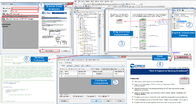
PSoC™ Creator is a free Windows-based Integrated Design Environment (IDE). It enables you to design hardware and firmware systems concurrently, based on PSoC™ 6 MCU. As Figure 2 shows, with PSoC™ Creator, you can
Procedure
- Browse collection of code examples from the File > Code Example… menu.
- Filter for examples based on Device family.
- Select from the menu of examples offered based on the Filter by options.
- Download the code example using the download button.
- Create a new project based on the selection.
- Explore the library of more than 100 components.
- Drag and drop components to build your hardware system design in the main design workspace.
- Review the component datasheets.
- Configure the components using configuration tools.
- Co-design your application firmware with the PSoC™ hardware.
Figure 2. PSoC™ Creator schematic entry and components
PSoC Creator help
Visit the PSoC™ Creator home page to download and install the latest version of PSoC™ Creator. Then launch PSoC™ Creator and navigate to the following items:
- Quick start guides: Choose Help > Documentation > Quick Start Guide. This guide gives you the basics for developing PSoC™ Creator projects
- Code examples: Choose File > Code Example or click the Find Code Example... link on the Start Page tab. These code examples demonstrate how to configure and use PSoC™ resources
- Component datasheets: Right-click a Component and select Open Datasheet. Visit the PSoC™ 6 MCU Component Datasheets page for a list of all Component datasheets
Peripheral Driver Library (PDL)
The PDL is the software development kit for PSoC™ 6 MCU devices. If you have experience working with PSoC™ devices but are new to PSoC™ 6 MCU, you will notice that PDL is the major addition to the development ecosystem.
Firmware developers who wish to work at the register level should also install the PDL. The PDL includes all the device-specific header files and startup code you need for your project. It also serves as a reference for each driver. Because the PDL is provided as source code, you can see how it accesses the hardware at the register level.
Some devices do not support particular peripherals. The PDL is a superset of all drivers for any supported device. This superset design means:
- All APIs needed to initialize, configure, and use a peripheral are available
- The PDL is useful across all PSoC™ 6 MCU devices, regardless of available peripherals
- The PDL includes error checking to ensure that the targeted peripheral is present on the selected device
This enables the code to maintain compatibility across platform as long as the peripherals are available. A device header file specifies the peripherals that are available for a device. If you write code that attempts to use an unsupported peripheral, you will get an error at compile time. Before writing code to use a peripheral, consult the datasheet for the particular device to confirm support for the peripheral.
PSoC™ Creator provides components that are based on PDL for your use with PSoC™ 6 MCU devices. This retains the essence of PSoC™ Creator in utilizing community-developed and pre-validated Components. However, the PDL is a source code library that you can use with any development environment.
The PDL includes the following key software resources:
- Header and source files for each peripheral driver
- Header and source files for middleware libraries
- Device-specific header, startup, and configuration files
- Template projects for supported third-party IDEs
Full documentation
The location for the documentation is <PDL install directory>\doc. There are two key documents.
The PDL v3.x user guide covers the fundamentals of working with the PDL, such as:
- Creating a custom project using the PDL (including third-party IDEs)
- Configuring a peripheral
- Managing pins in firmware
- Using the PDL as a learning tool for register-based programming
- Using the PDL API Reference documentation
The second key document is the PDL 3.x API reference manual.html. This reference has complete information on every driver in the PDL, including overview, configuration considerations, and details on every function, macro, data structure, and enumerated type
Support for other IDEs
You can also develop firmware for PSoC™ 6 MCU using your favorite IDE such as IAR Embedded Workbench. You can use the PDL with another IDE by using PSoC™ Creator to design the system and generate configuration code and then export to a target IDE.
See the AN219434 – PSoC™ 6 MCU Importing Generated Code into an IDE for details.
Using PSoC Creator to target another IDE
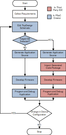
PSoC™ Creator sets up and configure PSoC™ 6 MCU system resources and peripherals. You then export the project to your IDE and continue developing firmware in your IDE. If there is a change in the device configuration, you edit the Topdesign schematic in PSoC™ Creator and regenerate the code for the target IDE. Figure 3 shows the workflow.
Figure 3. PSoC™ 6 MCU application development flowchart using PSoC™ Creator
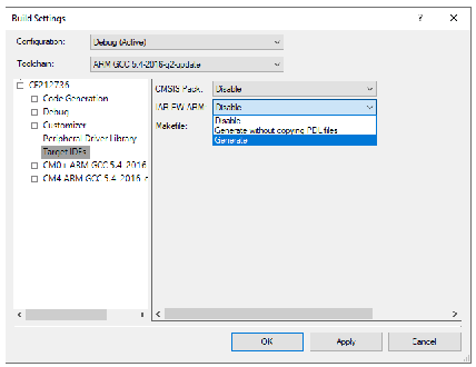
Code generated from PSoC™ Creator includes all required header, startup, and PDL files based on your design. Exporting the code generated from PSoC™ Creator is supported for Keil µVision, IAR Embedded Workbench, Eclipse-based IDEs, and for GNU-based command-line tools. You select your target IDE using the Project > Build Settings > Target IDEs panel. Enable the export package for your target IDE as shown in Figure 4. When you generate code, PSoC™ Creator also creates the corresponding export package.
Figure 4. Target IDE selection in project > Build settings
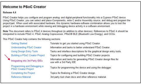
You then import the package into your IDE. The import details vary significantly per IDE. Consult the PSoC™ Creator Help to learn the process you must follow. Choose Help > PSoC™ Creator Help Topics. See Figure 5. The Integrating into 3rd Party IDEs topic points you to specific help files for each PSoC™ device family, and each supported IDE.
Figure 5. PSoC™ Creator help
You can work effectively in most if not all IDEs.If your IDE is not supported in the Target IDEs panel, you can still use PSoC™ Creator. After you generate code, add the necessary files directly to your IDE’s project. AN219434 – PSoC™ 6 MCU Importing generated code into an IDE provide detailed steps for manually importing the generated code into another IDE.
RTOS support
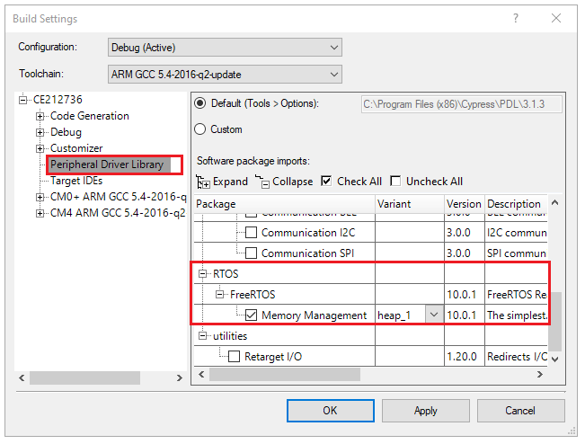
The PDL includes RTOS support for PSoC™ 6 MCU development: FreeRTOS source code is fully integrated and included with the PDL. You can import the FreeRTOS software package into your project by using the PSoC™ Creator RTOS import option. Navigate to Project > Build Settings menu and select FreeRTOS from the Software package imports option under Peripheral Driver Library > FreeRTOS as shown in Figure 6.
Figure 6. Import FreeRTOS in PSoC™ Creator project
If you have a preferred RTOS, use the resources provided as examples on how to integrate such code with the PDL.
Debugging
The CY8CKIT-062-BLE PSoC™ 6-BLE pioneer kit has the KitProg2 onboard programmer/debugger.
PSoC™ Creator supports debugging a single CPU (either CM4 or CM0+) at a time. Some third-party IDEs support multi-CPU debugging. For more information on debugging PSoC™ devices with PSoC™ Creator, see the PSoC™ Creator help. To update onboard programmer/debugger to Kitprog3, plug in your kit and open.
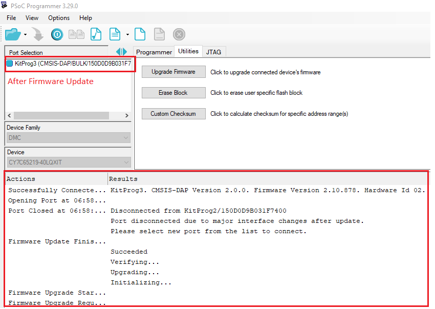
PSoC™ Programmer 3.29 tool. The tool automatically detects an older version of KitProg2 or KitProg3 on the kit and offers to upgrade the KitProg firmware to a newer version of KitProg3 as shown in Figure 7 and Figure 8.
Figure 7. Updating KitProg firmware

Figure 8. Firmware updates complete
CY8CKIT-062-BLE PSoC 6-BLE pioneer kit
CySmart Host Emulation Tool and mobile applications
The CySmart Host Emulation Tool is a Windows application that emulates a Bluetooth® LE central device using the PSoC™ 6-BLE pioneer kit’s Bluetooth® LE dongle. See CySmart Host Emulation Tool in Appendix D. IoT development tools for more information. Similar functionality is available in the CySmart mobile app for the iOS and Android devices. This tool is extremely useful in testing your Bluetooth® LE application.
Device features
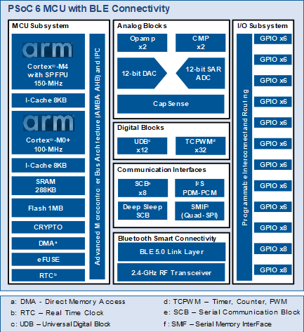
The PSoC™ 6-BLE device has an extensive feature set as shown in Figure 9. The following is a list of its major features. For more information, see the device datasheet, the Technical reference manual (TRM), and the section on Related application notes and code examples.
Figure 9. PSoC™ 6 MCU with Bluetooth® LE connectivity block diagram
32-bit dual-CPU MCU subsystem
- 150-MHz CM4 CPU with single-precision floating-point unit 100-MHz CM0+ CPU
- Up to 1 MB of user flash, with additional 32 KB for EEPROM emulation and 32 KB supervisory
- Up to 288 KB of SRAM with selectable Deep Sleep retention granularity at 32-KB retention boundaries
- Inter-processor communication supported in hardware
- Cryptography accelerators with support for hardware acceleration and true random number generator function
- Two 32-channel DMA controllers
- eFUSE: one-time programmable bits
- Uninterruptible secure boot with hardware hash-based authentication
I/O subsystem
- Up to 78 GPIOs that can be used for analog, digital, CAPSENSE™, or segment LCD functions
- Programmable drive modes, drive strength, and slew rates
- Two ports with smart I/Os that can implement boolean operations
Programmable analog blocks
- Two opamps of 6-MHz gain bandwidth (GBW), configurable as programmable gain amplifiers (PGA), comparators, or filters
- Two low-power comparators with less than 300 nA current consumption that are operational in Deep Sleep and Hibernate modes
- One 12-bit, 1-Msps SAR ADC with 16-channel sequencer
- One 12-bit voltage mode DAC
CAPSENSE™ with SmartSense™ auto-tuning
- Supports CAPSENSE™ Sigma-Delta (CSD) and CAPSENSE™ transmit/receive (CSX)
- Provides best-in-class SNR, liquid tolerance, and proximity sensing
Programmable digital blocks, Communication interfaces
- 12 UDBs for custom digital peripherals
- 32 TCPWM blocks configurable as 16-bit/32-bit timer, counter, PWM, or quadrature decoder
- Nine SCBs configurable as I2C master or slave, SPI master or slave, or UART
- Audio subsystem with one I2S interface and two PDM channels
- SMIF interface with support for execute-in-place from external quad SPI flash memory and on-the-fly encryption and decryption
Bluetooth® connectivity with Bluetooth® Low Energy 4.2
- 2.4-GHz Bluetooth® LE radio with integrated balun
- Bluetooth® 4.2 specification–compliant controller and host implementation
- Link layer engine that supports master/slave modes and up to four simultaneous connections
- Support for 2-Mbps LE data rate
Operating voltage range, power domains, and low-power modes
- Device operating voltage: 1.71 V to 3.6 V
- User-selectable core logic operation at either 1.1 V or 0.9 V
- Multiple on-chip regulators: low-drop out (LDO for Active, Deep Sleep modes), single input multiple output (SIMO) buck converter
- Active, Low-Power Active, Sleep, Low-Power Sleep, Deep Sleep, and Hibernate modes for fine power management
- Deep Sleep mode with operational Bluetooth® LE link: 4.5-µA typical current at 3.3 V with 64-KB SRAM retention
- An “always on” backup power domain with built-in RTC, power management integrated circuit (PMIC) control, and limited SRAM backup
Development setup
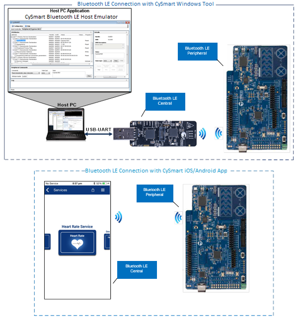
Figure 10 shows the hardware and software tools required for evaluating Bluetooth® LE peripheral designs using the PSoC™ 6-BLE device. In a typical use case, the PSoC™ 6-BLE pioneer kit (blue board in Figure 10) is configured as a Peripheral that can communicate with a Central device such as the CySmart iOS/Android app or CySmart Host Emulation Tool. The CySmart Host Emulation Tool also requires a Bluetooth® LE dongle (black board in Figure 10) for its operation. The PSoC™ 6-BLE pioneer kit includes a dongle.
Figure 10. Bluetooth LE functional setup
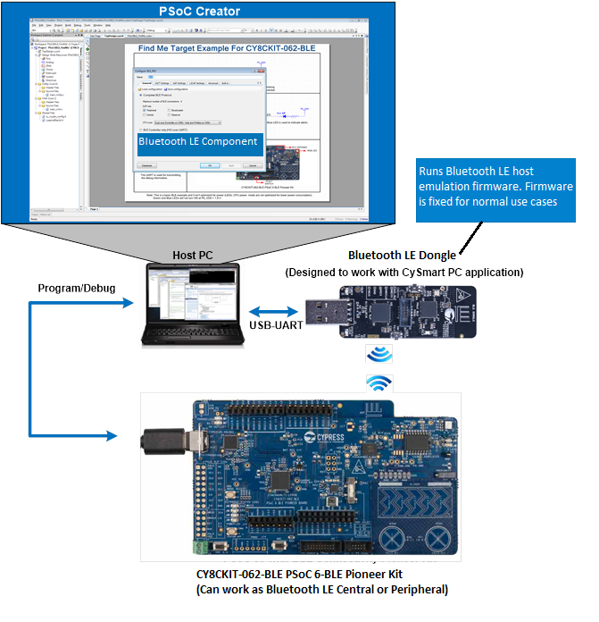
As shown in Figure 11, the Bluetooth® LE dongle is preprogrammed to work with the Windows CySmart Host Emulation Tool. The PSoC™ 6-BLE pioneer kit has an onboard USB programmer that works with PSoC™ Creator for programming or debugging your Bluetooth® LE design. The Bluetooth® LE pioneer kit can be powered over the USB interface. Both the Bluetooth® LE dongle and the Bluetooth® LE pioneer kit can be connected simultaneously to a common host PC for development and testing.
Figure 11. Bluetooth® LE development setup
My first PSoC 6 MCU design with Bluetooth LE
This section provides step-by-step instructions to build a simple design for the PSoC™ 6-BLE pioneer kit. A simple Bluetooth® SIG-defined standard profile called Find Me Profile (FMP) is implemented in the design. For creating advanced standard or custom Profile designs, refer to the Designing PSoC™ 6-BLE Applications and Creating a BLE Custom Profile application notes.
While the PSoC™ 6-BLE pioneer kit is intended to simplify and streamline design for Bluetooth® LE based applications, you can also use this setup to develop applications that do not use Bluetooth® LE.
Using the instructions
These instructions are grouped into several sections. Each section is devoted to a phase of the application development workflow. The major sections are:
- Part 1. Create a new project from scratch
- Part 2. Implement the design
- Part 3. Generate source code
- Part 4. Write the firmware
- Part 5. Build the project, program the Device
- Part 6. Test your design
These instructions require that you use a code example. However, the extent to which you use the code example depends on the path you choose to follow through these instructions.
We have defined three paths through these instructions:
| Path | Working from scratch code example as reference Only | Using code example new to PSoC™ Creator or Bluetooth® LE | Using code example familiar with PSoC™ Creator and Bluetooth® LE |
|---|---|---|---|
| Best For | Someone who wants hands-on experience to learn about PSoC™ Creator and/or Bluetooth® LE | Someone who is new to the tool or technology, and wants to see how it all works | Someone who knows the tools and technology, and wants to see it work on the PSoC™ 6 platform |
What you need to do for each path is clearly defined at the start of each part of the instructions.
If you start from scratch and follow all instructions in this application note, you use the code example as a reference while following the instructions. Working from scratch teaches you the most about the PSoC™ Creator design process, and how BLE works. This path also takes the most time.
You can also use the code example directly. It is a complete design, with all firmware written. You can walk through the instructions and observe how the steps are implemented in the code example. This is a particularly useful approach if you are already familiar with PSoC™ Creator and want to see how the Bluetooth® Low Energy Component is configured, for example. If you use the code example directly, you will be able to skip some steps.
In all cases, you should start by reading Before you begin and About the design.
Before you begin
Ensure that you have the following items installed on your host computer.
- PSoC™ Creator 4.4
- PDL v3.1.x
- The CySmart Host Emulation Tool or the CySmart iOS/Android app
- CE217236 – the code example used for this application note and
- The CY8CKIT-062-BLE PSoC™ 6-BLE pioneer kit with Kitprog3. Refer Debugging on how to update the Kitprog firmware
You can download the code example from the website by clicking the link above. You can also use the PSoC™ Creator File > Code Example command. Set the Device family to PSoC™ 63. Then set the Filter by option to Find Me. The CE212736_PSoC6BLE_FindMe code example appears. Select the code example, download by clicking on the download icon adjacent to the example. After installation is complete, click Create Project, and follow the on-screen instructions.
This design is developed for the CY8CKIT-062-BLE PSoC™ 6-BLE pioneer kit. If you wish to use other hardware, you must adapt the instructions to your needs.
About the design
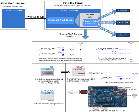
This design implements a Bluetooth® LE Find Me Profile (FMP) in the Target role that consists of an Immediate Alert Service (IAS). FMP and IAS are a Bluetooth® LE standard profile and service defined by the Bluetooth® SIG. Alert levels triggered by the Find Me Locator are indicated by varying the state of an LED on the Bluetooth® LE Pioneer Kit, as Figure 12 shows. In addition, two status LEDs indicate the state of the Bluetooth® LE interface. There is also an optional UART component to print debug messages to a terminal window.
Figure 12. My first PSoC™ 6-BLE design
Part 1. Create a new project from scratch
This part takes you step-by-step through the process of creating a project file from scratch.
| Path | Working from scratch code example as reference only | Using code example new to PSoC™ Creator or Bluetooth® LE | Using code example familiar with PSoC™ Creator and Bluetooth® LE |
|---|---|---|---|
| Actions | Perform all steps | Do Step 1 Read the rest of the steps | Do Step 1, then jump to Part 2 |
Launch PSoC™ Creator and get started.
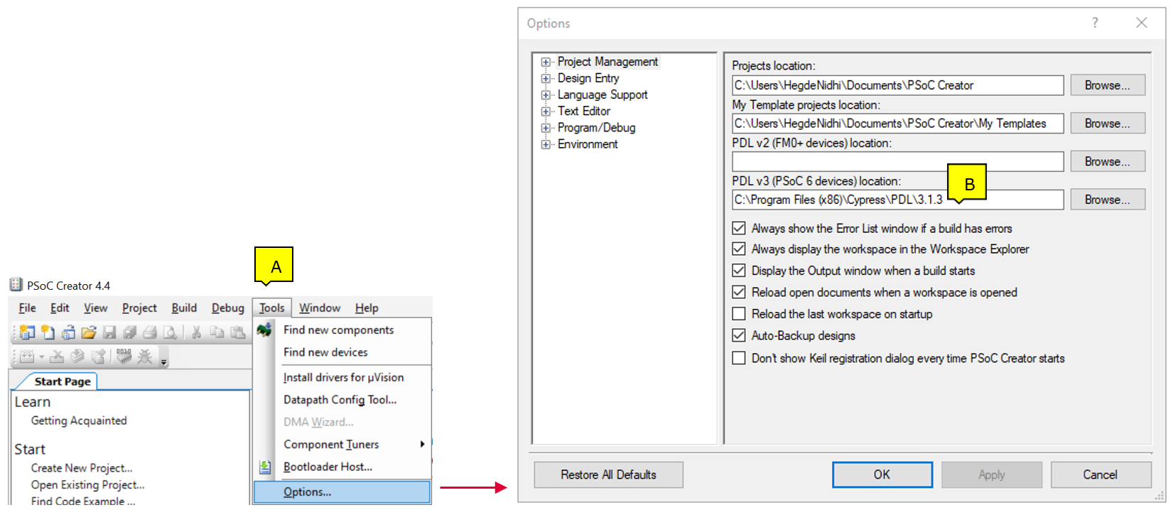
- Ensure that PSoC™ Creator can find the PDLAttention: This should be set correctly automatically during installation, but nothing works if this isn’t set up right. See Figure 13 for help with this step.
- Choose menu that is Tools > Options
- On the Project Management panel, check the path in the PDL v3 (PSoC™ 6 devices) location field
- Ensure that it is correct. If it is not, click Browse and locate the installed directory of the PDL. The default location is C:\Program Files (x86)\Cypress\PDL\3.0.1
Figure 13. Peripheral Driver Library (PDL) location
Optional: Jump to Part 2. Implement the design
- Create a new PSoC™ Creator project
- Choose File > New > Project, as Figure 14 shows. The Create Project window appears
Figure 14. Create a new PSoC™ Creator project
Figure 15. Open existing code example workspace
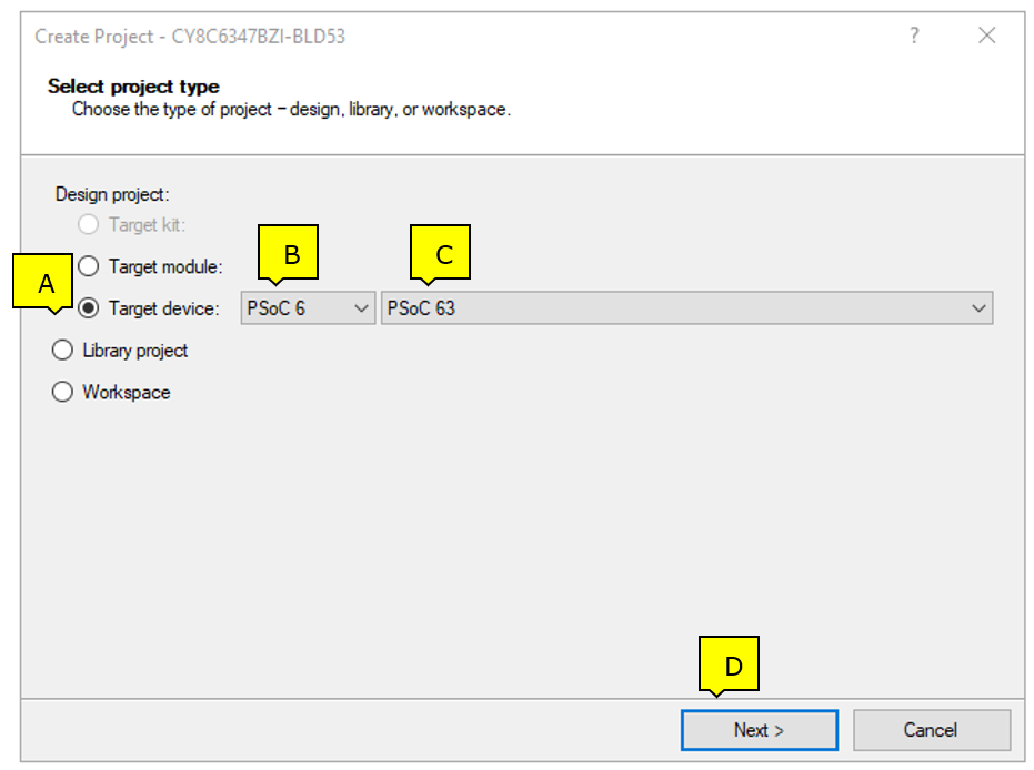
Select PSoC™ 6 Bluetooth® LE as the target device
Tip: PSoC™ Creator speeds up the development process by automatically setting various project options for specified development kits or target devices. See Figure 14 for help with this step.- Select Target device
- From the family drop-down list, select PSoC™ 6
- From the device drop-down menu, list PSoC™ 63
- Click Next. The Select project template panel appears
PSoC™ Creator uses CY8C6347BZI-BLD53 as the default device in the PSoC™ 6 MCU with Bluetooth® LE family. This device is mounted on the CY8CKIT-062-BLE PSoC™-BLE Connectivity Pioneer Kit.
If you are intending to use custom hardware based on PSoC™ 6-BLE, or a different PSoC™ 6-BLE part number, this is the place you choose to Launch device selector option in Target device and select the appropriate part number.
Figure 16. Selecting target device
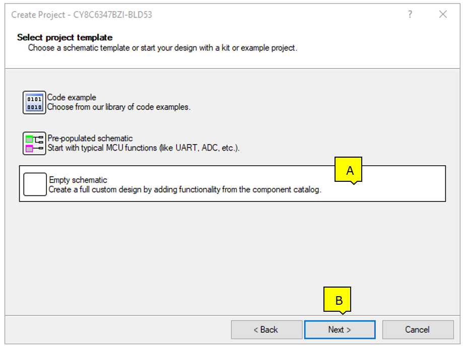
- Pick a project template
- Choose empty schematic
- Click Next
Figure 17. Pick a project template
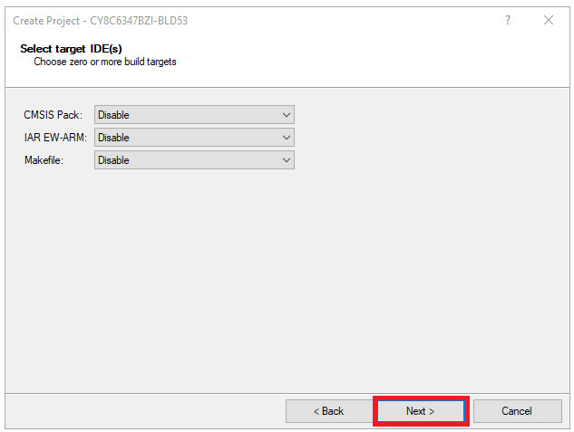
- Select target IDE(s)Note: If you expect to export the code from the project, specify the target IDE. By default, all export options are disabled. You can modify this setting later if circumstances change.
- Click Next to accept the default options
Figure 18. Select target IDEs (all disabled)
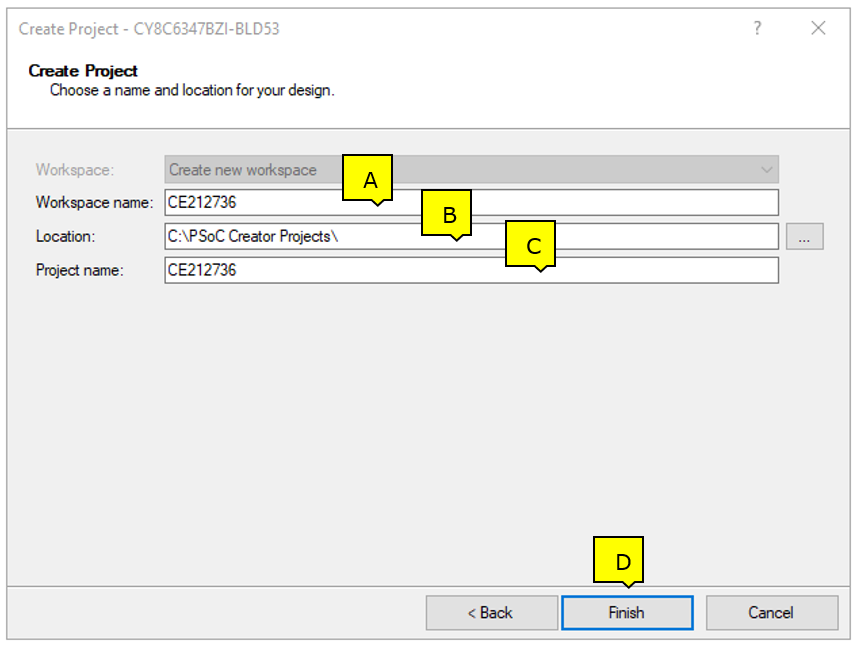
- Create the projectNote: In this step, you set the name and location for your workplace, and a name for the project. See Figure 19 for help with this step. A workspace is a container for one or more projects.
- Set the Workspace name
- Specify the Location of your workspace
- Set a Project name. The project and workspace names can be the same or different
- Click Finish
Figure 19. Project naming and location
You have successfully created a new PSoC™ Creator project.
Part 2. Implement the design
Now that you have a project file, it is time to implement the hardware design using PSoC™ Creator components. If you are using the code example directly, you already have a complete design. Perform the actions recommended based on your chosen path through this exercise.
| Path | Working from scratch code example as reference only | Using code example new to PSoC™ Creator or Bluetooth® LE | Using code example familiar with PSoC™ Creator and Bluetooth® LE |
|---|---|---|---|
| Actions | Perform all steps | Read and understand all steps | You can skip this part if you wish. Jump to Part 3. Generate source code |
Before you implement the design, a quick tour of the PSoC™ Creator interface is in order.
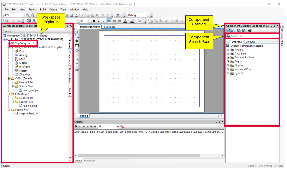
Figure 20 shows the PSoC™ Creator application displaying an empty design schematic.
The project includes a project folder with a base set of files. You view these files in the Workspace Explorer pane to the left. The project schematic opens by default. This is the TopDesign.cysch file. Double-click the file name in the explorer pane to open the schematic at any time. In a new project, the schematic is empty. If you are using the code example, this is the schematic for the Find Me Bluetooth® LE application.
The Component catalog is on the right side of the window. You can open it with the View > Component Catalog menu item. You can search for a Component by typing the name of the Component in the Search for… text box and then pressing the enter key. See Figure 20.
Figure 20. Schematic and component catalog
- Place components in the design
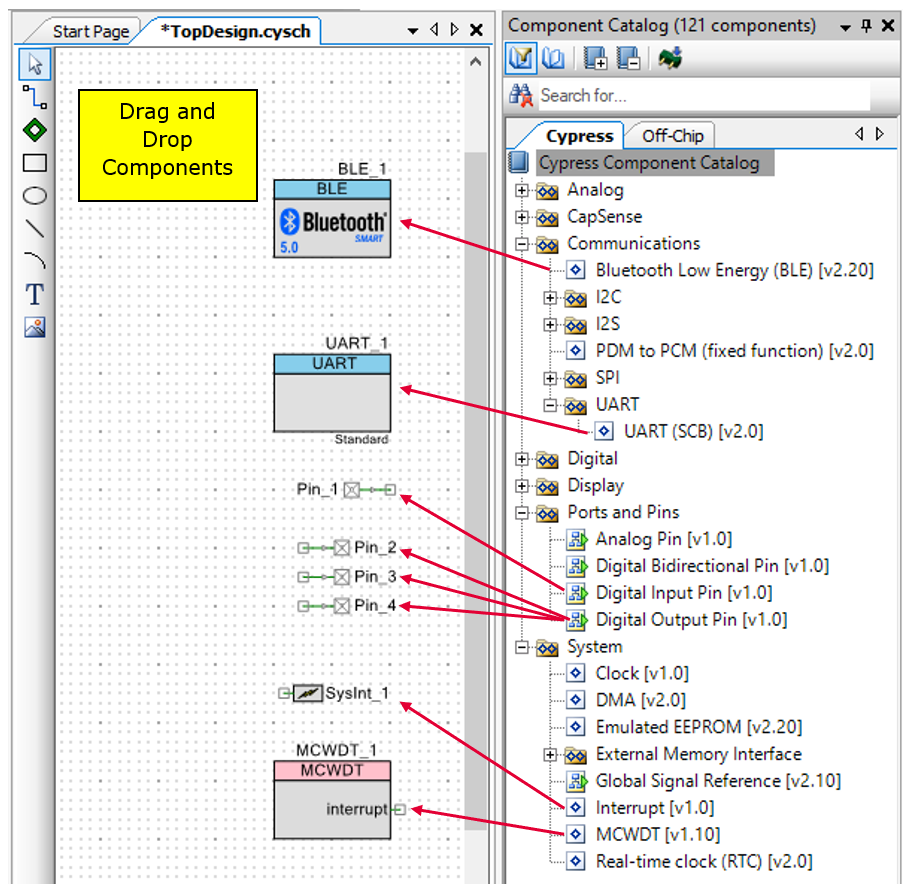
This design uses several components: the Bluetooth® Low Energy component, a digital input pin, three digital output pins, a UART, a Watchdog Timer, and an Interrupt. In this step, you add them to the design. You configure them in subsequent steps. Figure 21 shows the result.
- In the Component Catalog, expand the Communications group, drag a Bluetooth® Low Energy component into the schematic, and drop it. It doesn’t matter where you put a Component. Alternatively, you can search the Bluetooth® Low Energy Component by typing BLE in the Component Catalog search box
- Also in the Communications group, expand UART and drag a UART (SCB) Component into the design
- Expand the Ports and Pins group, drag a Digital Input Pin into the design
- From the same Ports and Pins group, drag a Digital Output Pin into the design. Repeat this twice, for a total of three pins
- Expand the System group, drag an Interrupt Component and a MCWDT Component into the design
Figure 21. Place components in the design
PSoC™ Creator gives each Component a default name and properties. Default values may or may not be suitable for any given design. In subsequent steps you modify the name and some of the properties.
- Configure the three LED pins
One pin drives the alert status LED. The other two drive the Bluetooth® LE advertising and disconnection indicator LEDs. An LED on the Bluetooth® LE pioneer kit is active LOW; that is, the logic high pin-drive state turns OFF the LED, and the logic low pin-drive state turns it ON.
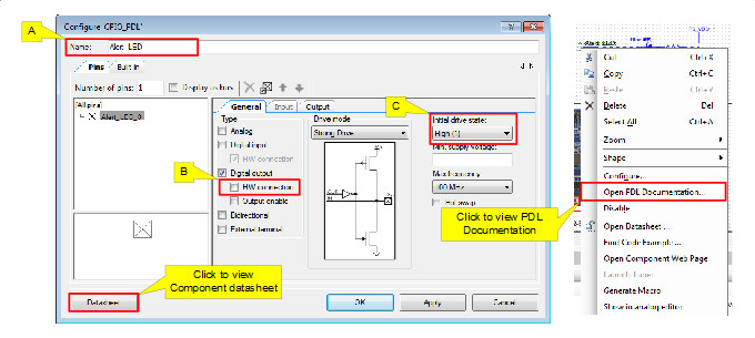
All three pins are configured identically, except for the name. Repeat these instructions three times, once for each pin. Figure 22 shows the configuration.
Double-click the component placed on the schematic to open the configuration dialog. Then perform the following steps.
- Change the name of the Component instance for each pin. The three names are Alert_LED, Advertising_LED and Disconnect_LED
- For each pin, deselectHW connection. The firmware will drive the pin
- For each pin, set Initial drive state to High (1). Hence, by default the LEDs will be OFF
Figure 22. Configuring an output pin component
Make sure you configure all three pins.
Figure 23. An output pin with off-chip components
- Configure the Hibernate wakeup pin
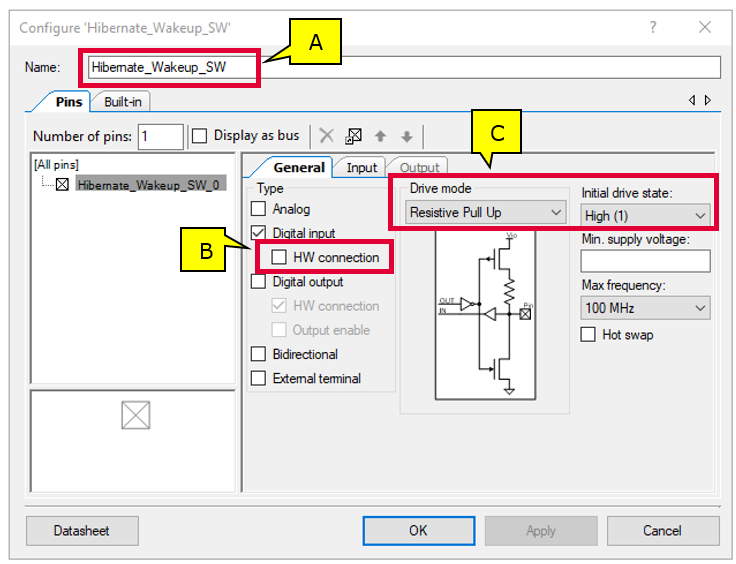
Switch SW2 on the Pioneer kit is connected to one of the Hibernate wakeup pins, P0[4] and when pressed pulls the port pin LOW. To configure this pin as the Hibernate wakeup switch, it must be configured as resistive pull up.
Figure 24 shows the configuration. Double-click the component placed on the schematic to open the configuration dialog, and then do the following:
- Change the name of the Component instance to Hibernate_Wakeup_SW
- Deselect HW connection. The firmware application firmware does not drive this pin. However, the pin is hard-wired to the Hibernate system. In the firmware, wakeup will be configured as active LOW
- Set Drive mode to Resistive Pull Up and Initial drive state to High (1). This will configure the device to detect the HIGH to LOW transition and wake up the device from Hibernate
Figure 24. Configuring an input pin component
- Configure the UART component
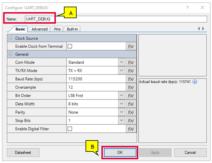
Double-click the component placed on the schematic to open the configuration window. The design uses this Component to display debug messages in a terminal window at a baud rate of 115200 bps. It is not related to Bluetooth® LE functionality.
- Change the Name of the Component instance to “UART_DEBUG”
- Click OK
The design uses default values for all other settings.
Figure 25. Configuring the SCB-based UART component
- Set the general Bluetooth® LE options
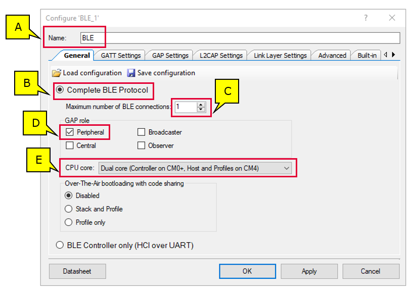
Double-click the Bluetooth® Low Energy Component placed on the schematic to open the configuration window. Set the General properties as shown in Figure 26. Except for the Component name and the stack operation, this application uses default general properties.
- Change the Name to “BLE”
- Confirm that Complete BLE Protocol is selected
- Change Maximum number of BLE connections to 1. This will configure the BLE stack appropriately
- Confirm that Peripheral is selected as the GAP role. This sets the device to act as a BLE Peripheral device and respond to Central device requests
- Select Dual core (Controller on CM0+, Host and Profiles on CM4) option for CPU core. This will split the Bluetooth® LE stack to work on both the cores. The CM0+ core runs the BLE controller portion of the stack and is responsible for maintaining the BLE connection. The BLE Host runs on the CM4 core and performs application-level tasks. The main advantage of this dual-CPU setup is that the CM4 core can go into Deep Sleep low-power mode when there are no Bluetooth® LE-related tasks pending
Figure 26. Bluetooth® Low Energy component general configuration
- Specify the Generic Attribute (GATT) settings
In this step, you set the Bluetooth® LE profile as shown in Figure 27.
- Click the GATT Settings tab to display GATT options
- Click the Add Profile drop-down menu
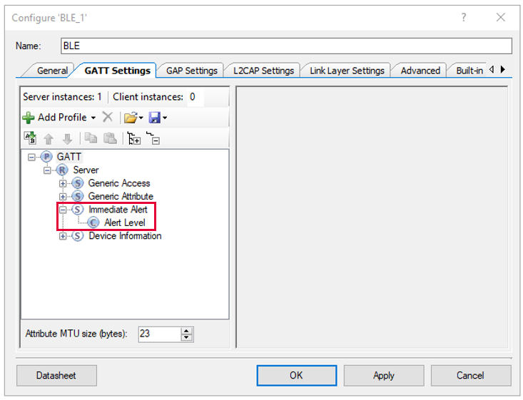
- Select the Find Me > Find Me Target (GATT Server) option. This sets the GAP Peripheral role profile. When the menu disappears, notice that a new service “Immediate Alert” appears, as shown in Figure 28
Figure 27. Bluetooth® Low Energy component immediate alert service added
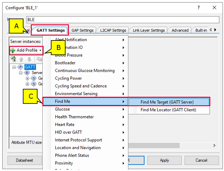
Figure 28. Bluetooth® Low Energy component immediate alert service added
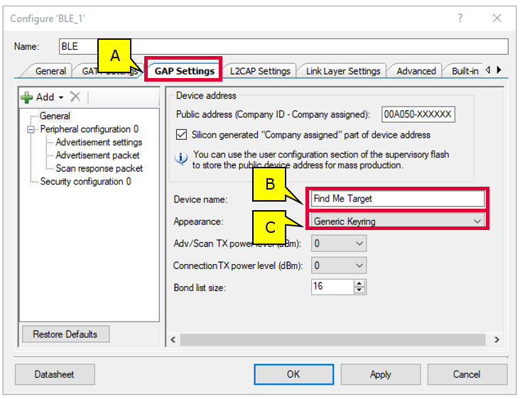
- Specify the Generic Access Profile (GAP) general settings
There is a series of panels to cover GAP settings. The left menu provides access to all the panels. See Figure 29.
- Click the GAP Settings tab to display GAP options. The General panel appears by default
- Enter Find Me Target as the Device name
- Set the Appearance to Generic Keyring
All other general settings use default values. This includes that the device uses Silicon generated “Company assigned” part of device address. This configures the device name and type that appears when a Host device attempts to discover your device, and then assigns a unique Bluetooth® LE device address to your device.
Figure 29. Bluetooth® Low Energy component general GAP settings
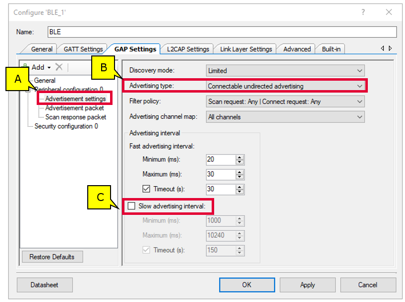
- Specify the GAP advertisement settings
See Figure 30 for help with this step.
- Click the Advertisement settings item in the left menu. The panel appears
- Set Advertising type to Connectable undirected advertising
- Deselect the Slow advertising interval checkbox
Other than that, default values work for this application. It uses limited discovery mode with an advertising timeout of 30 seconds and a fast advertisement interval of 20 to 30 ms. Fast advertising allows quick discovery and connection but consumes more power due to increased RF advertisement packets.
Figure 30. Bluetooth® Low Energy component GAP advertisement settings
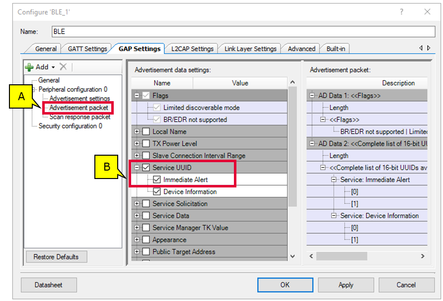
- Specify the GAP advertisement packet settings
In this step, you enable the device for the Immediate Alert Service (IAS). See Figure 31.
- Click the Advertisement packet item in the left menu. The panel appears
- Expand the Service UUID item, and select Immediate Alert
This configures the device to notify Bluetooth® Low Energy central devices that the IAS is available. As you add items, the structure and content of the advertisement packet appears to the right of the configuration panel.
Figure 31. Bluetooth® Low Energy component GAP advertisement packet settings
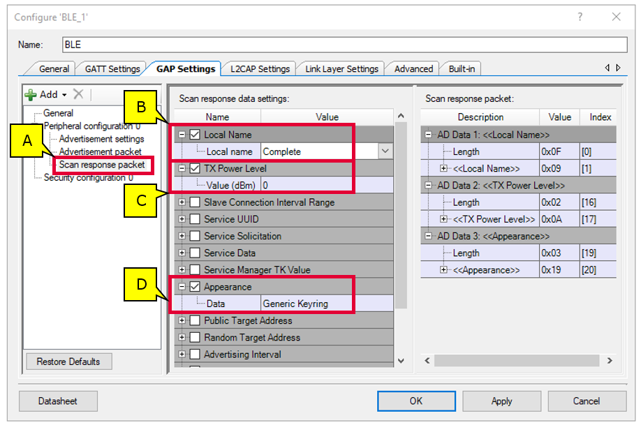
- Specify scan response packet settings
In this step, you specify the configuration for the Scan response packet. Figure 32 shows the result. Note that as you add values, the structure and content of the scan response packet appears to the right of the configuration panel.
- Click the Scan response packet item in the left menu. The panel appears
- Select Local Name to include that item in the response. The default setting of Complete is OK
- Select TX Power Level to include that item in the packet
- Select Appearance to include that item in the packet
Figure 32. Bluetooth® Low Energy component GAP scan response packet
- Specify security configuration settings
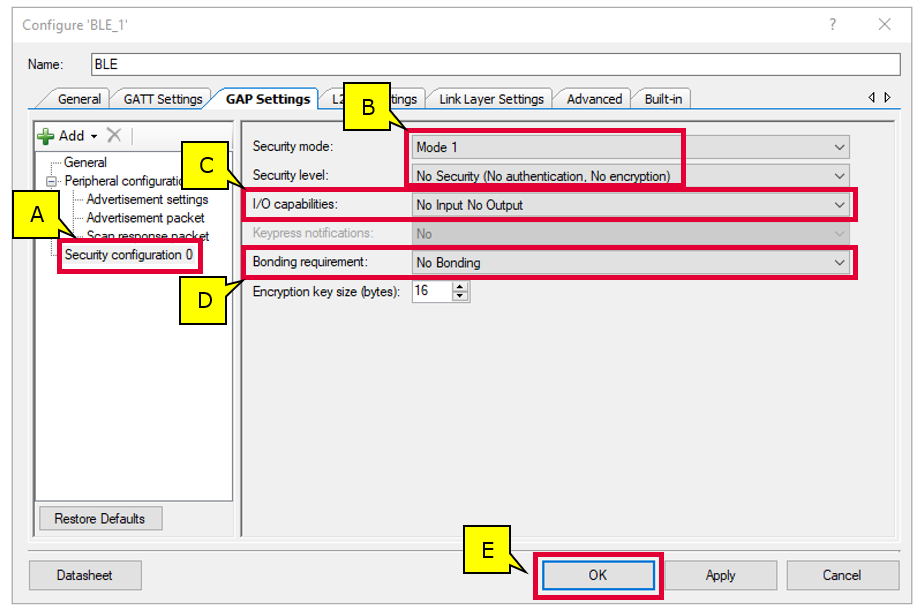
In this step, you configure security settings for the device. It uses a configuration that does not require authentication, encryption, or authorization for data exchange. See Figure 33.
- Click the Security configuration 0 item in the left menu. The panel appears
- Confirm that Security mode is Mode 1 and Security level is No Security. If not, modify the settings
- Set IO capabilities to No Input No Output
- Set Bonding requirement to No Bonding
- Click OK to complete the configuration of the Bluetooth® Low Energy Component Bluetooth® Low Energy Component
Figure 33. Bluetooth® Low Energy component GAP security settings
In this design, all other settings use default values, including all options in the LDCAP Settings, Link Layer Settings, and Advanced tabs.
See the Component datasheet to learn the significance of each setting.
- Configure the MCWDT Component to trigger an interrupt
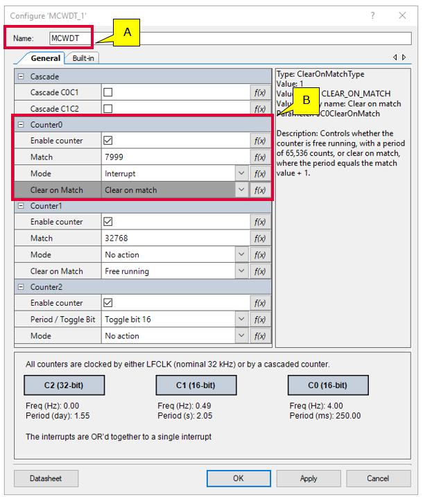
In this step, you configure the Multi-Counter Watchdog (MCWDT) Component to trigger an interrupt every 250 ms (4 Hz). The clock source of the MCWDT is the low frequency clock (LFCLK). The LFCLK’s source is the Internal Low Speed Oscillator (ILO) by default. The design will use this interrupt to blink the Alert LED at 2 Hz when a MILD alert is received. See Figure 34. Double click the Component placed on the schematic and configure as below.
- Change the Name to MCWDT
- For Counter0, change the Match value to 7999, Mode to Interrupt. Set the Clear on Match field to Clear on match
- Click OK to complete the configuration of the MCWDT Component
Figure 34. MCWDT_PDL settings
- Configure the interrupt Component to wake up the CM4 CPU in Deep Sleep mode
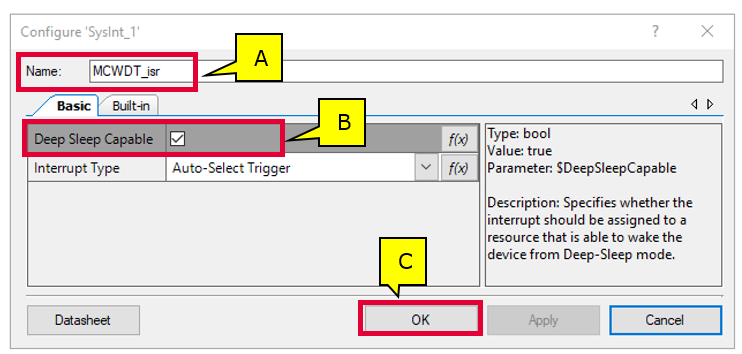
In this step, you configure the SysInt Component to wake up the CM4 CPU. See Figure 35.
- Change the Name to MCWDT_isr
- Select the interrupt to be Deep Sleep Capable
- Click OK to complete the configuration of the SysInt Component
Figure 35. SysInt_PDL settings
As a final step, connect the interrupt output of the MCWDT Component to MCWDT_isr Component input. This routes the watchdog interrupt to the CPU (the selection of the CM4 CPU for this interrupt will be set in the system interrupt configuration in a later step). In the schematic, use the wire tool button or press the W key to start wiring the components.
Figure 36. Connect MCWDT peripheral interrupt to CM4 CPU
- Set the physical pins for each pin component
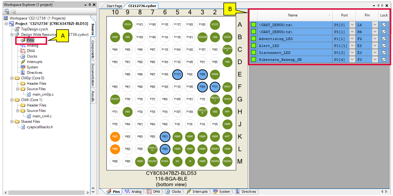
One task remains to complete the design. You must associate each component with the required physical pins on the device. The choice of which pin to use is driven by the board design. You can find this information in the kit schematic. Figure 37 shows the end result of this step.
To set a pin, type either the port number or pin number in the corresponding field, or use the drop-down menu to pick the port or pin. Typically, the port number is used instead of the pin number since these names are independent of the specific package being used.
- Open the pin selector
In the Workspace Explorer pane, double-click the Pins item under the Design wide resources. The pin selector for this device appears.
- Set each pin as shown in Table 1
| Pin component name | Port name |
|---|---|
| UART_DEBUG:rx | P5[0] |
| UART_DEBUG:tx | P5[1] |
| Advertising_LED | P1[1] |
| Alert_LED | P11[1] |
| Disconnect_LED | P0[3] |
| Hibernate_Wakeup_SW | P0[4] |
Figure 37. Pin assignment
- System clock configuration
The design uses default values for the high frequency system clock settings. Although you do not modify high frequency clocks for this design, you should know how PSoC™ Creator manages them. If you are working with your own board, you may need to modify these clocks.
In this step, you set the low frequency clock source to be the accurate watch crystal oscillator (WCO) on the board. This clock is used by the Bluetooth® Low Energy Subsystem (BLESS) for timing purposes.
- In the Workspace Explorer pane, double-click the Clocks item under Design Wide Resources (CE212736.cydwr). The list of clocks appears
- Click Edit Clock… and the Configure System Clocks dialog appears
- Here you can see the clock tree, and modify the clocks as required. Note that there are tabs for different types of clocks such as Source Clocks, FLL/PLL, High Frequency Clocks, and Miscellaneous Clocks
- Click the Source Clocks tab
- Enable the BLE ECO by selecting the checkbox in the AltHF BLE ECO block. The parameters should match the crystal used on the board. For the CY8CKIT-062-BLE kit, the ECO Frequency is 32 MHz, and Accuracy is ±50 ppm. There are no load caps on the board and hence use the minimum specified Load cap (pF) of 9.900. Ensure that the Startup Time (µs) is 785 µs for a quick startup of the ECO crystal
- Enable the WCO clock by selecting the checkbox in the WCO (32.768 kHz) block
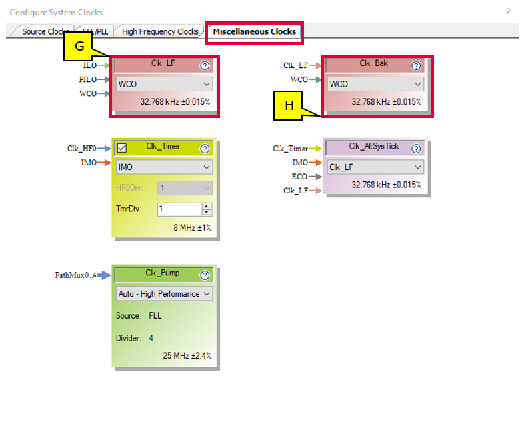
- Click the Miscellaneous Clocks tab
- Select WCO to be the source for LFClk
- Select WCO to be the source for BakClk
Figure 38. Clock configuration - source clocks
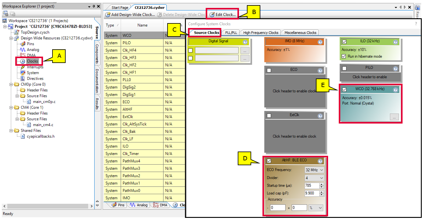
Figure 39. Clock configuration - miscellaneous clocks
- System interrupt configuration
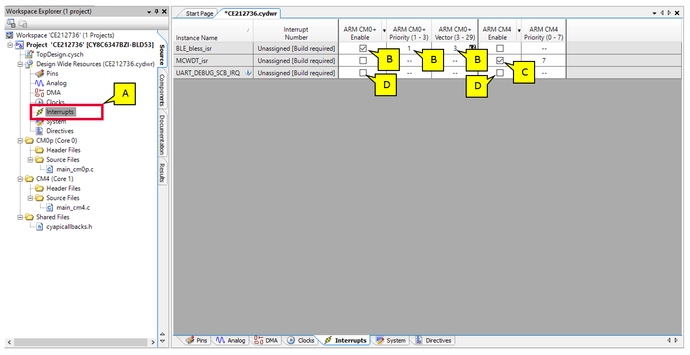
In this step, you configure the system interrupts. See Figure 40.
- In the Workspace Explorer pane, double-click the Interrupts item under Design Wide Resources. The list of interrupts appears
- Confirm that the BLE_bless_isr is enabled for the CM0+ CPU, the priority is set to 1, and vector is set to 3. This ensures that the Bluetooth® LE controller interrupts are handled by CM0+ at the highest priority, and in Deep Sleep mode as well
- Enable MCWDT_isr for CM4
- Disable the UART_DEBUG_SCB_IRQ interrupt for both cores
- Deselect the corresponding checkboxes. You can ignore the interrupt related to UART_DEBUG Component because the design does not use it
The interrupt numbers are generated automatically by PSoC™ Creator when you generate the code in Part 3. Generate source code.
Figure 40. Interrupt configuration
The next part in the development process is to generate code.
Part 3. Generate source code
PSoC™ Creator generates source code based upon the design. The recommended workflow is to generate code before writing firmware. PSoC™ Creator will automatically create macros, constants, and API calls that you may then use in your firmware.
This part of the exercise is very simple, and the path is the same for everyone.
| Path | Working from scratch code example as reference only | Using code example new to PSoC™ Creator or Bluetooth® LE | Using code example familiar with PSoC™ Creator and Bluetooth® LE |
|---|---|---|---|
| Actions | Perform the one step | Perform the one step | Perform the one step |
- Generate the application
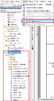
Choose Build > Generate application. PSoC™ Creator generates source code based on the design and puts the files in the Generated_Source folder. See Figure 41. PSoC™ Creator will alert you to errors or problems that may occur. If you are working from scratch and encounter errors, revisit the configuration steps in Part 2. Implement the design to ensure you have performed them correctly.
Figure 41. Generate application
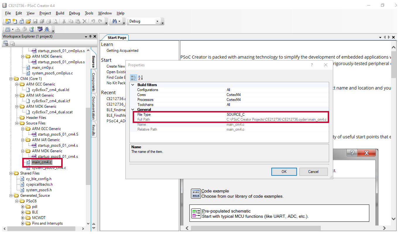
Background: PSoC™ 6-BLE is a dual-CPU platform. You can target firmware to run either on CM4 or CM0+. You set this at the source file level by accessing the file properties. Right-click a source file and select Properties.
Figure 41 shows the Properties dialog window. This code example targets the CM4 core.
By default, the main_cm0p.c file is targeted to CM0+ and the main_cm4.c file is targeted to CM4. You do not need to modify the properties for any other file. They are already set in the code example.
By convention, files targeted to run on the CM0+ are in the CM0p folder and files targeted to run on CM4 are in the CM4 folder, but the properties must also be set appropriately – just putting a file in the correct folder does not cause it to run on a specific core.
Figure 42. Setting target processor for a source C file
Part 4. Write the firmware
At this point in the development process you have created a project, implemented a hardware design, and generated code. In this part, you examine the firmware that implements Bluetooth® LE functionality in the application.
The firmware must accomplish several tasks to implement a Bluetooth® LE standard profile application, including:
- Perform system initialization
- Implement a BLE stack event handler
- Implement a BLE service-specific event handler
- Provide the main loop
- Implement low-power performance (optional)
The steps in this part discuss the firmware for the design that you configured in Part 2. Implement the design. The steps do not examine every single line of code but point out important elements in the code that implement significant functionality.
| Path | Working from scratch code example as reference only | Using code example new to PSoC™ Creator or Bluetooth® LE | Using code example familiar with PSoC™ Creator and Bluetooth® LE |
|---|---|---|---|
| Actions | Perform all steps | Skip step one Perform all other steps | Skip this part if you wish. Jump to Part 5. Build the project, program the Device |
The code example has all the required code. If you are working from scratch, in step one you copy the source files from the code example project. If you are using the code example, those files are already in your project, so you can skip step one.
- Add files to your project
If you are using the code example, you can skip this step. The code example already has the required source files.
If you are working from scratch, the required source code files are not in your project.
- Locate the CE212736.cydsn folder, which contains the source files for the code example. The folder is in the Code Example workspace archive that you downloaded earlier
Copy these files from the CE212736.cydsn folder to your project’s .cydsn folder. Replace any existing files
- BLEFindMe.h
- debug.h
- LED.h
- BLEFindMe.c
- debug.c
- main_cm0p.c
- main_cm4.c
Add these files to your project. You can do this by dragging them from the Windows folder onto the Workspace explorer, and dropping them in the CM4 folder location in the workspace. See Figure 43
- BLEFindMe.h
- debug.h
- LED.h
- BLEFindMe.c
- debug.c
Figure 43. Add files to your project
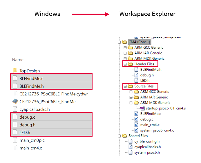
You do not have to add main_cm0p.c or main_cm4.c. The project has these files by default. You just replaced them in the project folder, so the project will use the newer version you just copied.
- Initialize the system
In the remaining steps, we examine code in the main_cm0p.c and main_cm4.c file. The code snippets frequently have the debugging print statements removed for clarity. See the actual source file for a complete understanding of the code.
Figure 44 shows the steps in the process of initializing the system. When the PSoC™ 6-BLE device is reset, the firmware first performs system initialization, which includes setting up the CPU cores for execution, enabling global interrupts, and enabling other Components used in the design. The initialization is split across the CPU cores. The CM0p CPU comes out of reset and attempts to start the Bluetooth® LE controller part. If it is successful, the CM0p CPU then enables CM4 CPU. The CM4 CPU will start the Bluetooth® LE host part and register the necessary application side handler functions.
Figure 44. System initialization flowchart – CM4
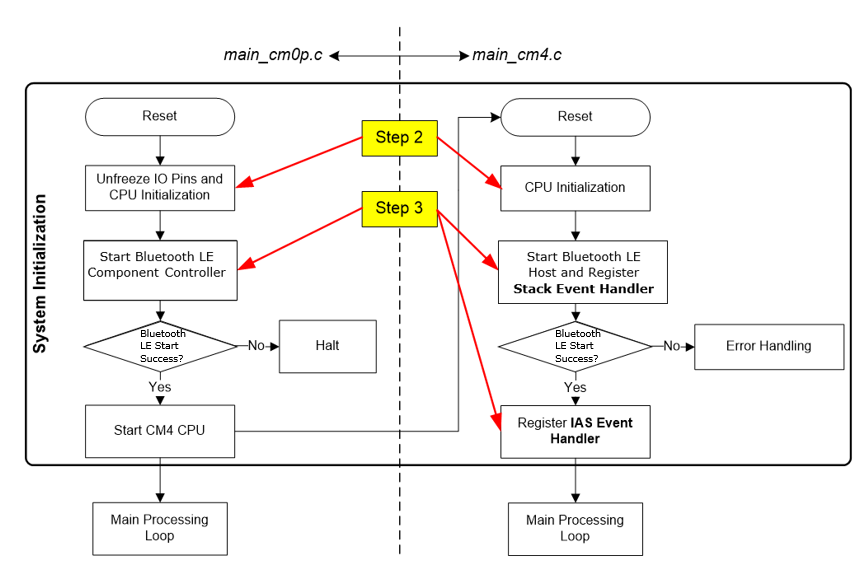
The code in main_cm0p.c declares a local variable to hold the return value from Bluetooth® LE API calls. The key task is to enable the Bluetooth® LE controller, and set up the CM4 for the application code to run. In the main loop, the CM0p CPU processes the Bluetooth® LE events pending on the controller. In case of no pending events, the CM0p enters Deep Sleep mode.
int main(void)
(
  cy_en_ble_api_result_t          apiResult;
  __enable_irq();    /* Enable global interrupts. */
  /* Unfreeze IO if device is waking up from hibernate */
  if(Cy_SysPm_GetIoFreezeStatus())
  (
    Cy_SysPm_IoUnfreeze();
  )
  /* Start the Controller portion of BLE. Host runs on the CM4 */
  apiResult = Cy_BLE_Start(NULL);
  if(apiResult == CY_BLE_SUCCESS)
  (
    /* Enable CM4 only if BLE Controller started successfully.
    * CY_CORTEX_M4_APPL_ADDR must be updated if CM4 memory layout
    * is changed. */
    Cy_SysEnableCM4(CY_CORTEX_M4_APPL_ADDR);
  )
  else
  (
    /* Halt CPU */
    CY_ASSERT(0u != 0u);
  )
  for(;;)
  (
    /* Place your application code here. */
    /* Put CM0p to deep sleep. */
    Cy_SysPm_DeepSleep(CY_SYSPM_WAIT_FOR_INTERRUPT);

    /* Cy_Ble_ProcessEvents() allows BLE stack to process pending events */
    /* The BLE Controller automatically wakes up host if required */
    Cy_BLE_ProcessEvents();
)
The code in main_cm4.c initializes the key Components to be used by the CM4 and continuously runs a Bluetooth® LE application process. The BleFindMe_Init() routine initializes and starts all the Components, including setting up the CM4 interrupt. It performs the key task of enabling the Bluetooth® LE host.
In the application process, the CM4 CPU processes the Bluetooth® LE events pending on the host. If there are no events pending, the CM4 enters Deep Sleep low-power mode.
int main(void)
(
  __enable_irq(); /* Enable global interrupts. */

  /* Initialize BLE */
  BleFindMe_Init();

  for(;;)
  (
    BleFindMe_Process();
  )
)
- Start the Bluetooth® Low Energy component and register the event handlers
After the CPUs are initialized, the firmware initializes the Bluetooth® Low Energy component, which sets up the complete Bluetooth® LE subsystem. The BleFindMe_Init() subroutine handles the work. To focus on the key tasks, debug print statements have been removed. Examine the source file to see the full code.
As a part of the Bluetooth® Low Energy Bluetooth® Low Energy component initialization, you must pass the event handler function, which will be called by the Bluetooth® LE stack to notify of pending events. If the Bluetooth® Low Energy component initializes successfully, the firmware registers a second event handler for events specific to the IAS.
The code uses PDL API function calls to configure the application. First it starts the Bluetooth® Low Energy Component. The parameter is the address of the stack event handler function.
The code also gets the stack version. In case the debug port is enabled, the version is printed in the serial communication window.
It then registers the IAS event handler to handle Immediate Alert Service related events. Finally, it configures and enables the MCWDT to trigger interrupts once every 250 ms.
void BleFindMe_Init(void)
(
  cy_en_ble_api_result_t apiResult;
  cy_stc_ble_stack_lib_version_t stackVersion;

  /* Configure switch SW2 as hibernate wake up source */
  Cy_SysPm_SetHibWakeupSource(CY_SYSPM_HIBPIN1_LOW);

  /* Start Bluetooth® Low Energy Component and register generic event handler */
  apiResult = Cy_BLE_Start(StackEventHandler);
  apiResult = Cy_BLE_GetStackLibraryVersion(&stackVersion);


  /* Register IAS event handler */
  Cy_BLE_IAS_RegisterAttrCallback(IasEventHandler);

  /* Enable 4 Hz free-running MCWDT counter 0*/
  /* MCWDT_config structure is defined by the MCWDT_PDL component based
     on parameters entered in the customizer. */
  Cy_MCWDT_Init(MCWDT_HW, &MCWDT_config);
  Cy_MCWDT_Enable(MCWDT_HW, CY_MCWDT_CTR0, 93 /* 2 LFCLK cycles */);

  /* Unmask the MCWDT counter 0 peripheral interrupt */
  Cy_MCWDT_SetInterruptMask(MCWDT_HW, CY_MCWDT_CTR0);

  /* Configure ISR connected to MCWDT interrupt signal*/
  /* MCWDT_isr_cfg structure is defined by the SYSINT_PDL component based
     on parameters entered in the customizer. */
  Cy_SysInt_Init(&MCWDT_isr_cfg, &MCWDT_Interrupt_Handler);

  /* Clear CM4 NVIC pending interrupt for MCWDT */
  NVIC_ClearPendingIRQ(MCWDT_isr_cfg.intrSrc);

  /* Enable CM4 NVIC MCWDT interrupt */
  NVIC_EnableIRQ(MCWDT_isr_cfg.intrSrc);
)
- Implement the stack event handler
The Bluetooth® LE stack within the Bluetooth® Low component generates events. These events provide status and data to the application firmware through the Bluetooth® LE stack event handler. Figure 45 shows a simplified flowchart representing certain events.
Figure 45. BLE stack event handler flowchart
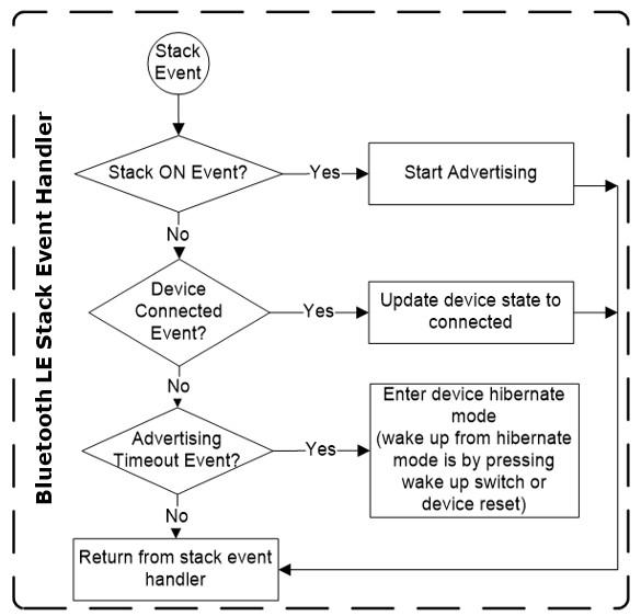
The event handler must handle a few basic events from the stack. For the Find Me Target application in this code example, the BLE stack event handler must process the events described in Table 2. The actual code recognizes and responds to additional events, but they are not mandatory for this application.
| Bluetooth® LE stack event name | Event description | Event handler action |
|---|---|---|
| CY_BLE_EVT_STACK_ON | Bluetooth® LE stack initialization is completed successfully | Start advertisement and reflect the advertisement state on the LED |
| CY_BLE_EVT_GAP_DEVICE_DISCONNECTED | Bluetooth® LE link with the peer device is disconnected | Restart advertisement and reflect the advertisement state on the LED |
| CY_BLE_EVT_GAP_DEVICE_CONNECTED | Bluetooth® LE link with the peer device is established | Update the BLE link state on the LED |
| CY_BLE_EVT_GAPP_ADVERTISEMENT_START_STOP | Bluetooth® LE stack advertisement start/stop event | Shutdown the Bluetooth® LE stack |
| CY_BLE_EVT_HARDWARE_ERROR | Bluetooth® LE hardware error | Update the LED status to reflect a hardware error and halt the CPU |
| CY_BLE_EVT_STACK_SHUTDOWN_COMPLETE | BLE stack has been shut down | Configure the device in Hibernate mode and wait for event on wakeup pin |
The code snippets show two examples of how the event handler responds to an identified event. See the actual source code for a complete understanding.
In this snippet, the handler responds to the “advertisement start/stop” event. The code toggles the LEDs appropriately. If advertisement has started, the advertisement LED turns on. The disconnect LED turns off, because the device started advertisement and is ready for a connection. If advertising is stopped, the code sets the LEDs appropriately, and sets a flag to enter Hibernate mode.
/* This event indicates peripheral device has started/stopped advertising */
case CY_BLE_EVT_GAPP_ADVERTISEMENT_START_STOP:
  DEBUG_PRINTF("CY_BLE_EVT_GAPP_ADVERTISEMENT_START_STOP: ");
  if(Cy_BLE_GetAdvertisementState() == CY_BLE_ADV_STATE_ADVERTISING)
  (
    DEBUG_PRINTF("Advertisement started \r\n");
    Cy_GPIO_Write(Advertising_LED_0_PORT, Advertising_LED_0_NUM, LED_ON);
    Cy_GPIO_Write(Disconnect_LED_0_PORT, Disconnect_LED_0_NUM, LED_OFF);
  )
  else if(Cy_BLE_GetAdvertisementState() == CY_BLE_ADV_STATE_STOPPED)
  (
    DEBUG_PRINTF("Advertisement stopped \r\n");
    Cy_GPIO_Write(Advertising_LED_0_PORT, Advertising_LED_0_NUM, LED_OFF);
    Cy_GPIO_Write(Disconnect_LED_0_PORT, Disconnect_LED_0_NUM, LED_ON);


    /* Advertisement event timed out before connection, shutdown BLE
     * stack to enter hibernate mode and wait for device reset event
     * or SW2 press to wake up the device */
    Cy_BLE_Stop();
  )
break;
In this snippet, the handler responds to the “disconnected” event. It sets the LEDs correctly, and sets the Hibernate flag.
These snippets give you a sense for how the event handler responds to events. Examine the actual function to see how each event is handled.
/* This event is generated when disconnected from remote device or
failed to establish connection. */

case CY_BLE_EVT_GAP_DEVICE_DISCONNECTED:
  if(Cy_BLE_GetConnectionState(appConnHandle) == CY_BLE_CONN_STATE_DISCONNECTED)
  (
    DEBUG_PRINTF("CY_BLE_EVT_GAP_DEVICE_DISCONNECTED %d\r\n", CY_BLE_CONN_STATE_DISCONNECTED);
    alertLevel = CY_BLE_NO_ALERT;
    Cy_GPIO_Write(Advertising_LED_0_PORT, Advertising_LED_0_NUM, LED_OFF);
    Cy_GPIO_Write(Disconnect_LED_0_PORT, Disconnect_LED_0_NUM, LED_ON);

    /* Enter into discoverable mode so that remote device can search it */
    apiResult = Cy_BLE_GAPP_StartAdvertisement(CY_BLE_ADVERTISING_FAST, CY_BLE_PERIPHERAL_CONFIGURATION_0_INDEX);
    if(apiResult != CY_BLE_SUCCESS)
    (
      DEBUG_PRINTF("Start Advertisement API Error: %d \r\n", apiResult);
      ShowError();

      /* Execution does not continue beyond this point */
    )
    else
    (
      DEBUG_PRINTF("Start Advertisement API Success: %d \r\n", apiResult);
      Cy_GPIO_Write(Advertising_LED_0_PORT, Advertising_LED_0_NUM, LED_ON);
      Cy_GPIO_Write(Disconnect_LED_0_PORT, Disconnect_LED_0_NUM, LED_OFF);
    )
  )
break;
- Implement the service-specific event handler
The Bluetooth® Low Energy Component also generates events corresponding to each of the services supported by the design. For the Find Me Target application, the Bluetooth® Low Energy Component generates IAS events that let the application know that the Alert Level characteristic has been updated with a new value. The event handler gets the new value and stores it in the variable alertLevel. The main loop toggles the alert LED based on the current alert level.
Figure 46 shows the IAS event handler flowchart.
Figure 46. Bluetooth® LE IAS event handler flowchart
The code snippet shows how the firmware accomplishes this task.
void IasEventHandler(uint32 event, void *eventParam)
(

  /* Alert Level Characteristic write event */
  if(event == CY_BLE_EVT_IASS_WRITE_CHAR_CMD)
  (
    /* Read the updated Alert Level value from the GATT database */
    Cy_BLE_IASS_GetCharacteristicValue(CY_BLE_IAS_ALERT_LEVEL,
         sizeof(alertLevel), &alertLevel);
  )

  /* To remove unused parameter warning */
  eventParam = eventParam;
)
- Process events as they occur (main loop)
The main loop simply calls BleFindMe_Process(). Figure 47 shows the BleFindMe_Process() flowchart.
Figure 47. Firmware main loop flowchart
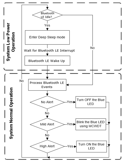
If there are no pending Bluetooth® LE host events and there is no active interaction, the application goes into low-power mode. It then tells the Bluetooth® LE to process events, and updates the LEDs based on the alert level.
        /* The call to EnterLowPowerMode also causes the device to enter hibernate mode if the BLE is disconnected. */

  EnterLowPowerMode();
  /* Cy_Ble_ProcessEvents() allows BLE stack to process pending events */
  Cy_BLE_ProcessEvents();
  /* Update Alert Level value on the Blue LED */
  switch(alertLevel)
  (
    case CY_BLE_NO_ALERT:
      /* Disable MCWDT interrupt at NVIC */
      NVIC_DisableIRQ(MCWDT_isr_cfg.intrSrc);
      /* Turn the Blue LED OFF in case of no alert */
      Cy_GPIO_Write(Alert_LED_0, LED_OFF);
      break;

/* Use the MCWDT to blink the Blue LED in case of mild alert */
case CY_BLE_MILD_ALERT:
    /* Enable MCWDT interrupt at NVIC */
    NVIC_EnableIRQ(MCWDT_isr_cfg.intrSrc);
    /* The MCWDT interrupt handler will take care of LED blinking */
    break;
case CY_BLE_HIGH_ALERT:
    /* Disable MCWDT interrupt at NVIC */
    NVIC_DisableIRQ(MCWDT_isr_cfg.intrSrc);
    /* Turn the Blue LED ON in case of high alert */
    Cy_GPIO_Write(Alert_LED_0, LED_ON);
    break;
/* Do nothing in all other cases */
default:
    break;
)
This completes the summary of how the firmware works in the code example. Feel free to explore the source files for a deeper understanding.
Part 5. Build the project, program the Device
This section shows how to program the PSoC™ 6-BLE device. If you are using a development kit with a built-in programmer (the CY8CKIT-062-BLE PSoC™ 6-BLE Pioneer Kit, for example), connect the board to your computer using the USB cable. If you are developing on your own hardware, you may need a hardware programmer/debugger; for example, a CY8CKIT-002 MiniProg3.
| Path | Working from scratch code example as reference only | Using code example new to PSoC™ Creator or Bluetooth® LE | Using code example familiar with PSoC™ Creator and Bluetooth® LE |
|---|---|---|---|
| Actions | Perform all steps | ||
If you are working from scratch and encounter errors, revisit prior steps to ensure that you accomplished all the required tasks. You can work to resolve errors or switch to the code example for these final steps.
- Select the debug target
PSoC™ Creator can debug one core at a time.
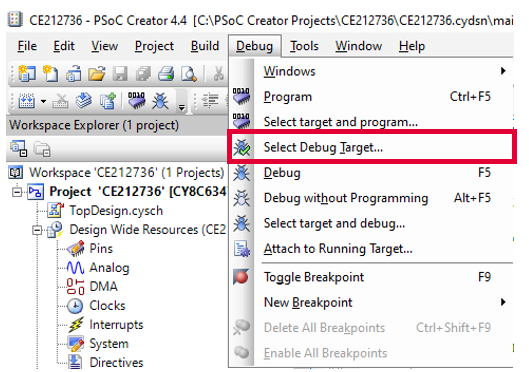
- In PSoC™ Creator, choose Debug > Select Debug Target, as Figure 48 shows
Figure 48. Selecting debug target
- Connect to the board
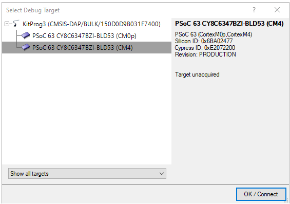
In the Select Debug Target dialog box, select the CM4 target, then click OK or Connect, as Figure 49 shows.
Figure 49. Connecting to a device
- Program the board
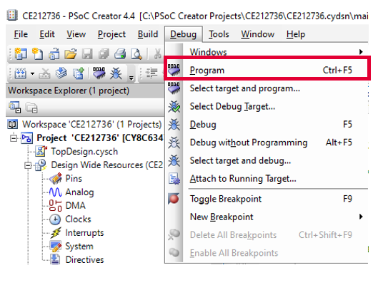
Choose Debug > Program to program the device with the project, as Figure 50 shows.
Figure 50. Programming the device
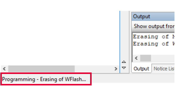
You can view the programming status in the lower left corner of the window PSoC™ Creator window, as Figure 51 shows.
Figure 51. Programming status
In a dual core application, the linker files put each executable at the correct location in memory. Execution begins on the CM0+ core, which enables the CM4 core.
When programming is complete, the application runs. The LED turns green, indicating that the target is advertising. After the advertising timeout occurs it turns red, indicating that it is disconnected.
Part 6. Test your design
This section describes how to test your Bluetooth® LE design using either the CySmart mobile app or the CySmart Host Emulation Tool. The setup for testing your design using the Bluetooth® LE Pioneer Kit is shown in Figure 10.
| Path | Working from scratch code example as reference only | Using code example new to PSoC™ Creator or Bluetooth® LE | Using code example familiar with PSoC™ Creator and Bluetooth® LE |
|---|---|---|---|
| Actions | Perform either step 1 or step 2 | ||
- Test using the CySmart Mobile App
- Turn on Bluetooth® on your iOS or Android device
- Launch the CySmart app
- Press the reset switch on the Bluetooth® LE Pioneer Kit to start Bluetooth® LE advertisements from your design. The green LED must be on for the CySmart app to see the device
- Pull down the CySmart app home screen to start scanning for BLE Peripherals. The Find Me target appears as a Bluetooth® LE device in the CySmart app home screen. Tap to establish a Bluetooth® LE connection. If the phone does not find the target, press the reset button again, or try the CySmart Host Emulation tool (step 2)
- Select the “Find Me” Profile from the carousel view
- Select an Alert Level value on the Find Me Profile screen and watch the state of the blue LED on your device change per your selection
Figure 52 shows this process using the iOS app. Figure 53 shows the process using the Android app.
Figure 52. Testing with CySmart iOS App
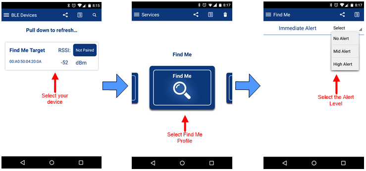
Figure 53. Testing with CySmart Android App

- Test using the CySmart Host Emulation Tool
As an alternative to the CySmart mobile app, you can use the CySmart Host Emulation Tool to establish a Bluetooth® LE connection with your design and perform read or write operations on Bluetooth® LE characteristics.
- If not already installed, install the CY Smart Host Emulation Tool
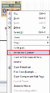
Right-click the Bluetooth® Low Energy Component symbol on the Top Schematic and select Download CySmart as shown in Figure 54. Follow the installer directions to install the tool.
Figure 54. Download CySmart
- Connect the Bluetooth® LE dongle to your Windows personal computer. Wait for the driver installation to be completed
- Launch the CySmart Host Emulation Tool
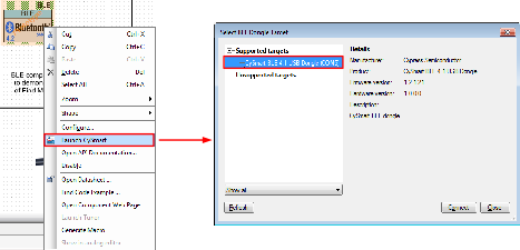
The tool automatically detects the Bluetooth® LE dongle. Click Refresh if the Bluetooth® LE dongle does not appear in the Select BLE Dongle Target pop-up window. Click Connect, as shown in Figure 55.
Figure 55. CySmart Bluetooth® LE dongle selection
- Click Configure Master Settings and then click Restore Defaults, as shown in Figure 56. Then, click OK
Figure 56. CySmart master settings configuration
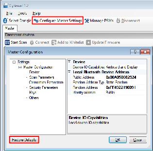
- Press the reset switch on the Bluetooth® LE pioneer kit to start BLE advertisements from your design. The LED turns green to indicate you are advertising
- On the CySmart Host Emulation Tool, click Start Scan. Your device name (configured as Find Me Target) should appear in the Discovered devices list, as shown in Figure 57
Figure 57. CySmart device discovery

- Select Find Me Target and click Connect to establish a Bluetooth® LE connection between the CySmart Host Emulation Tool and your device, as shown in Figure 58
Figure 58. CySmart device connection

- Once connected, switch to the Find Me Target device tab and discover all the attributes on your design from the CySmart Host Emulation Tool, as shown in Figure 59
Figure 59. CySmart attribute discovery

- Scroll down the Attributes window and locate the Immediate Alert Service fields. Write a value of 0, 1, or 2 to the Alert Level characteristic under the Immediate Alert Service, as Figure 60 shows. Observe the state of the LED on your device change per your Alert level characteristic configuration
Figure 60. Testing with CySmart Host Emulation Tool
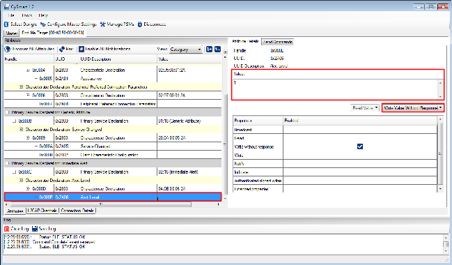
- When you are finished exploring, click the Disconnect button in the CySmart application. The LED turns red to indicate you are disconnected
You can repeat this process by pressing the reset button on the board to resume advertising.
Summary
This application note explored the PSoC™ 6-BLE device architecture and the associated development tools.
PSoC™ 6-BLE is a truly programmable embedded system-on-chip, integrating low-power Bluetooth® LE radio, configurable analog and digital peripheral functions, memory, and a dual-CPU system on a single chip. The integrated features and low-power modes make PSoC™ 6-BLE an ideal choice for battery-operated wearable, health, and fitness Bluetooth® LE applications.
Related application notes and code examples
For a complete and updated list of PSoC™ 6 MCU code examples, please visit our code examples webpage. For more PSoC™ 6 MCU related documents, visit our PSoC™ 6 MCU product webpage.
Table 3 lists the system-level and general application notes that are recommended for the next steps in learning about PSoC™ 6-BLE and PSoC™ Creator.
| Document | Document name |
|---|---|
| AN221774 | Getting Started with PSoC™ 6 MCU on PSoC™ Creator |
| CE221773 | PSoC™ 6 MCU Hello World Example |
| AN218241 | PSoC™ 6 MCU Hardware Design Considerations |
| AN219434 | PSoC™ 6 MCU Importing Generated Code into an IDE |
| AN219528 | PSoC™ 6 MCU Low-Power Modes and Power Reduction Techniques |
Table 4 lists the application notes and code examples (CE) for specific peripherals and applications of the device.
| Document | Document name |
|---|---|
| Programmable digital | |
| Bluetooth® smart | |
| AN91162 | Creating a BLE Custom Profile |
| AN91445 | Antenna Design and RF Layout Guidelines |
| AN92584 | Designing for Low Power and Estimating Battery Life for BLE applications |
| CE218463 | Bluetooth® Low Energy (BLE) Alert Notification Client/Server |
| CE218464 | Bluetooth® Low Energy (BLE) Phone Alert Client/Server |
| System resources, CPU, and interrupts | |
| AN215656 | PSoC™ 6 MCU Dual-CPU System Design |
| AN217666 | PSoC™ 6 MCU Interrupts |
| CE216795 | PSoC™ 6 MCU Dual-CPU Basics |
| CE216825 | PSoC™ 6 MCU Real-Time Clock Basics |
| CE218129 | PSoC™ 6 MCU Wake up from Hibernate Using Low-Power Comparator |
| CE218541 | PSoC™ 6 MCU Fault-Handling Basics |
| CE218542 | PSoC™ 6 Custom Tick Timer Using RTC Alarm Interrupt |
| CE218552 | PSoC™ 6 MCU UART to Memory Buffer Using DMA |
| CE218964 | PSoC™ 6 MCU RTC Daily Alarm |
| CE219339 | PSoC™ 6 MCU MCWDT and RTC Interrupts (Dual Core) |
| CE219521 | PSoC™ 6 MCU GPIO Interrupt |
| CE219881 | PSoC™ 6 MCU Switching Power Modes |
| CE220060 | PSoC™ 6 MCU Watchdog Timer |
| CE220061 | PSoC™ 6 MCU Multi-Counter Watchdog Interrupts |
| CE220120 | PSoC™ 6 MCU Blocking Mode Flash Write |
| CE220169 | PSoC™ 6 MCU Periodic Interrupt Using TCPWM |
| GPIO | |
| CE219490 | PSoC™ 6 Breathing LED Using SMART IO |
| CE219506 | PSoC™ 6 Clock Buffer Using SMART IO |
| CE220263 | PSoC™ 6 MCU GPIO Pins Example |
| CAPSENSE™ | |
| AN92239 | Proximity Sensing with CAPSENSE™ |
| AN85951 | PSoC™ 4 and PSoC™ 6 MCU CAPSENSE™ Design Guide |
| SMIF | |
| Bootloader | |
| AN213924 | MCU Bootloader Software Development Kit (SDK) Guide |
| CE213903 | PSoC™ 6 MCU Basic Bootloaders |
| Communications | |
| CE220541 | PSoC™ 6 MCU SCB EzI2C |
| Segment LCD | |
| Audio | |
| CE218636 | PSoC™ 6 MCU Inter-IC Sound (I2S) Example |
| CE219431 | PSoC™ 6 MCU PDM-to-PCM Example |
| RTOS | |
| CE217911 | PSoC™ 6 FreeRTOS™ Example Project |
| Security | |
| CE220465 | PSoC™ 6 MCU Cryptography – AES Demonstration |
| CE220511 | PSoC™ 6 MCU Cryptography – SHA Demonstration |
Appendix A. Glossary
This section lists the most commonly used terms that you might encounter while working with PSoC™ family of devices.
Component Customizer: Simple GUI in PSoC™ Creator that is embedded in each Component. It is used to customize the Component parameters and is accessed by right-clicking a Component.
Components: Components are used to integrate multiple ICs and system interfaces into one PSoC™ Component that is inherently connected to the MCU via the main system bus. For example, the Bluetooth® Low Energy component creates Bluetooth® Smart products in minutes. Similarly, you can use the Programmable Analog components for sensors.
MiniProg3: Programming hardware for development that is used to program PSoC™ devices on your custom board or PSoC™ development kits that do not support a built-in programmer.
PSoC™: A programmable, embedded design platform that includes one or more CPUs, such as the 32-bit CM4, with both analog and digital programmable blocks. It accelerates embedded system design with reliable, easy-to-use solutions, such as touch sensing, and enables low-power designs.
PSoC™ Creator: PSoC™ 3, PSoC™ 4, PSoC™ 5LP, and PSoC™ 6-BLE IDE software that installs on your PC and allows concurrent hardware and firmware design of PSoC™ systems, or hardware design followed by export to other popular IDEs.
Peripheral Driver Library: The Peripheral Driver Library (PDL) simplifies software development for the PSoC™ 6 MCU architecture. The PDL reduces the need to understand register usage and bit structures, thus easing software development for the extensive set of peripherals available.
PSoC™ Programmer: A flexible, integrated programming application for programming PSoC™ devices. PSoC™ Programmer is integrated with PSoC™ Creator to program PSoC™ 3, PSoC™ 4, PRoC, PSoC™ 5LP, and PSoC™ 6 MCU designs.
Appendix B. Bluetooth LE protocol
Overview
BLE, also known as Bluetooth® Smart, was introduced by the Bluetooth® SIG as a low-power wireless standard operating in the 2.4-GHz ISM band. Figure 61 shows the BLE protocol stack.
Figure 61. Bluetooth® LE architecture
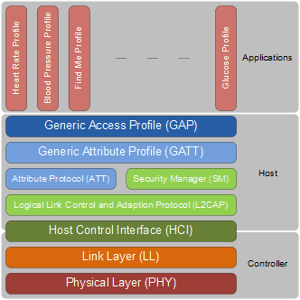
The BLE stack can be subdivided into three groups:
- Controller: A physical device that encodes the packet and transmits it as radio signals. On reception, the controller decodes the radio signals and reconstructs the packet
- Host: A software stack consisting of various protocols and Profiles (Security Manager, Attribute Protocol, and so on) that manages how two or more devices communicate with one another
- Application: A use case that uses the software stack and the controller to implement a particular functionality
The following sections provide an overview of the multiple layers of the Bluetooth® LE stack, using the standard Heart Rate and Battery Service as examples. For a detailed Bluetooth® LE architecture description, see the Bluetooth® Core Specification.
Physical Layer (PHY)
The physical layer transmits or receives digital data at 1 Mbps using Gaussian frequency-shift keying (GFSK) modulation in the 2.4-GHz ISM band. The Bluetooth® LE physical layer divides the ISM band into 40 RF channels with a channel spacing of 2 MHz, 37 of which are data channels and 3 are advertisement channels.
Link Layer (LL)
The link layer implements key procedures to establish a reliable physical link (using an acknowledgement and flow-control-based architecture) and features that help make the Bluetooth® LE protocol robust and low-power. Some link layer functions include:
- Advertising, scanning, creating, and maintaining connections to establish a physical link
- 24-bit CRC and AES-128-bit encryption for robust and secure data exchange
- Establishing fast connections and low-duty-cycle advertising for low-power operation
- Adaptive Frequency Hopping (AFH), which changes the communication channel used for packet transmission so that the interference from other devices is reduced
At the link layer, two roles are defined:
- Master: A smartphone is an example that configures the link layer in the master configuration
- Slave: A heart-rate monitor device is an example that configures the link layer in the slave configuration
PSoC™ 6-BLE devices can operate in either configuration.
The link-layer slave is the one that advertises its presence to another link-layer master. A link-layer master receives the advertisement packets and can choose to connect to the slave based on the request from an application (see Figure 62). In this example implementation of a heart-rate monitor application, a heart-rate monitor device acts as the slave and sends the data to a smartphone, which acts as the master. A smartphone app then can display the reading on the smartphone.
PSoC™ 6-BLE devices implement the time-critical and processor-intensive parts of the link layer such as advertising, CRC, and AES encryption in hardware. Link-layer control operations such as entering the advertisement state and starting encryption are implemented in firmware.
Figure 62 shows the Bluetooth® LE link-layer packet structure and sizes of the individual fields in the link-layer packet. The link-layer packet carries all upper layer data in its payload field. It has a 4-byte access address that is used to uniquely identify communications on a physical link, and ignore packets from a nearby Bluetooth® LE device operating in the same RF channel. 24-bit CRC provides data robustness.
Figure 62. Bluetooth® LE link layer protocol

Host Control Interface (HCI)
The HCI is the standard-defined interface between the host and the controller. It allows the host and the controller to exchange information such as commands, data, and events over different physical transports such as USB or UART. The HCI requires a physical transport only when the controller and the host are different devices.
In PSoC™ 6-BLE devices, the HCI is just a firmware protocol layer that passes the messages and events between the controller and the host.
Logical Link Control and Adaptation protocol (L2CAP)
L2CAP provides protocol multiplexing, segmentation, and reassembly services to upper-layer protocols. Segmentation breaks the packet received from the upper layer into smaller packets that the link layer can transmit, while reassembly combines the smaller packets received from the link layer into a meaningful packet. The L2CAP layer supports three protocol channel IDs for Attribute protocol (ATT), and L2CAP control, as shown in Figure 63. Bluetooth 4.2 allows direct data channels through the L2CAP connection-oriented channels on top of these protocol channels.
The L2CAP and the layers above it are implemented in firmware in PSoC™ 6-BLE.
Figure 63. Bluetooth® LE L2CAP layer
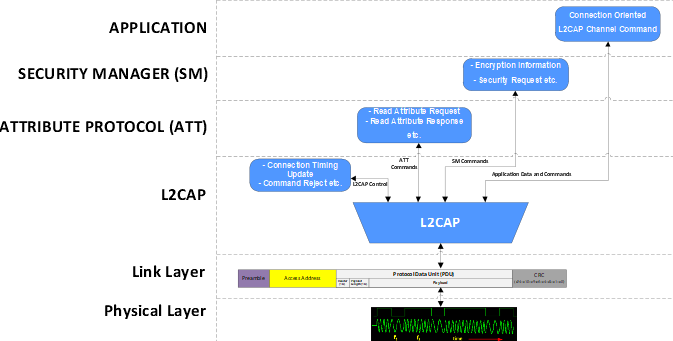
Security manager (SM)
The SM layer defines the methods used for pairing, encryption, and key distribution.
- Pairing is the process to enable security features. In this process, two devices are authenticated, the link is encrypted, and then the encryption keys are exchanged. This enables the secure exchange of data over the Bluetooth® LE interface without being snooped on by a silent listener on the RF channel
- Bonding is the process in which the keys and the identity information exchanged during the pairing process are saved. After devices are bonded, they do not have to go through the pairing process again when reconnected
Bluetooth® LE uses 128-bit AES for data encryption.
Attribute protocol (ATT)
There are two GATT roles in BLE that you should know to understand the ATT and GATT layers:
- GATT Server: A GATT Server contains the data or information. It receives requests from a GATT Client and responds with data. For example, a heart-rate monitor GATT Server contains heart-rate information; a BLE HID keyboard GATT Server contains user key press information
- GATT Client: A GATT Client requests and/or receives data from a GATT Server. For example, a smartphone is a GATT Client that receives heart-rate information from the heart-rate GATT Server; a laptop is a GATT Client that receives key-press information from a Bluetooth® LE keyboard
ATT forms the basis of Bluetooth® LE communication. This protocol enables the GATT Client to find and access data or attributes on the GATT Server. For more details about the GATT Client and Server architecture, see Generic Attribute Profile (GATT).
An attribute is the fundamental data container in the ATT/GATT layer, which consists of the following:
- Attribute handle: The 16-bit address used to address and access an attribute
- Attribute type: This specifies the type of data stored in an attribute. It is represented by a 16-bit UUID defined by the Bluetooth® SIG
For example, the 16-bit UUID of the Heart-Rate Service is 0x180D; the UUID for the Device Name Attribute is 0x2A00. Visit the Bluetooth® webpage for a list of 16-bit UUIDs assigned by the SIG.
- Attribute value: This is the actual data stored in the attribute
- Attribute permission: This specifies the attribute access, authentication, and authorization requirements. Attribute permission is set by the higher layer specification and is not discoverable through the attribute protocol
Figure 64 shows the structure of a Device name attribute as an example.
Figure 64. Attribute format example

Attribute hierarchy
Attributes are the building blocks for representing data in ATT/GATT. Attributes can be broadly classified into the following two groups to provide hierarchy and abstraction of data:
Characteristic: A collection of attributes that exposes the system information or meaningful data. A Characteristic consists of the following attributes:
- Characteristic declaration attribute: This defines the beginning of a characteristic
- Characteristic value attribute: This holds the actual data
- Characteristic descriptor attributes: These are optional attributes, which provide additional information about the characteristic value
“Battery Level” is an example of a characteristic in the Battery Service (BAS). Representing the battery level in percentage values is an example of a characteristic descriptor.
Figure 65 shows the structure of a characteristic with Battery Level as an example.
- The first part of a characteristic is the declaration of the characteristic (it marks the beginning of a characteristic) indicated by the Battery Level Characteristic in Figure 65
- Next is the actual characteristic value or the real data, which in the case of the Battery Level Characteristic is the current battery level. The battery level is expressed as a percentage of full scale, for example “65,” “90,” and so on
- Characteristic descriptors provide additional information that is required to make sense of the characteristic value. For example, the Characteristic Presentation Format Descriptor for Battery Level indicates that the battery level is expressed as a percentage. Therefore, when “90” is read, the GATT Client knows this is 90 percent and not 90 mV or 90 mAh. Similarly, the Valid Range Characteristic descriptor (not shown in Figure 65) indicates that the battery level range is between 0 and 100 percent
- A Client Characteristic Configuration Descriptor (CCCD) is another commonly used Characteristic descriptor that allows a GATT Client to configure the behavior of a Characteristic on the GATT Server. When the GATT Client writes a value of 0x01 to the CCCD of a Characteristic, it enables asynchronous notifications (described in the next section) to be sent from the GATT Server. In the case of a Battery Level Characteristic, writing 0x01 to the Battery Level CCCD enables the Battery Service to notify its battery level periodically or on any change in battery-level value
Figure 65. Characteristic format and example
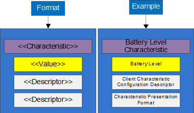
- Service: The type of attribute that defines a function performed by the GATT Server. A service is a collection of characteristics and can include other services. The concept of a service is used to establish the grouping of relative data and provide a data hierarchy. See Figure 66 for an example of a Heart Rate Service (HRS).
A service can be of two types: A primary service or a secondary service. A primary service exposes the main functionality of the device, while the secondary service provides additional functionality. For example, in a heart-rate monitoring device, the HRS is a primary service and BAS is a secondary service.
A service can also include other services that are present on the GATT Server. The entire included services become part of the new service.
Figure 66. Bluetooth® LE Heart rate service example
The word “Profile” in Bluetooth® LE is a collection of services and their behavior that together perform a particular end application. A Heart Rate Profile (HRP) is an example of a Bluetooth® LE Profile that defines all the required services for creating a heart-rate monitoring device. See the Generic Access Profile (GAP) section for details.
Figure 67 shows the data hierarchy using attributes, characteristics, services, and profiles defined previously in this section.
Figure 67. Bluetooth® LE data hierarchy
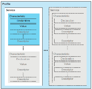
Attribute operations
Attributes defined in the previous section are accessed using the following five basic methods:
- Read request: The GATT Client sends this request to the GATT Server to read an attribute value. For every request, the GATT Server sends a response to the GATT Client. A smartphone reading the Battery-Level Characteristic of a heart-rate monitor device (see Figure 65) is an example of a Read Request
- Write request: The GATT Client sends this request to the GATT Server to write an attribute value. The GATT Server responds to the GATT Client, indicating whether the value was written. A smartphone writing a value of 0x01 to the CCCD of a Battery Level characteristic to enable notifications is an example of a Write Request
- Write command: The GATT Client sends this command to the GATT Server to write an attribute value. The GATT Server does not send any response to this command. For example, the Bluetooth® LE Immediate Alert Service (IAS) uses a Write Command to trigger an alert (turn on an LED, ring a buzzer, drive a vibration motor, and so on) on an IAS Target device (for example, a Bluetooth® LE key fob) from an IAS locator (for example, a smartphone)
- Notification: The GATT Server sends this to the GATT Client to notify it of a new value for an attribute. The GATT Client does not send any confirmation for a notification. For example, a heart-rate monitor device sends heart-rate measurement notifications to a smartphone when its CCCD is written with a value of 0x01
- Indication: The GATT Server sends this type of message. The GATT Client always confirms it. For example, a Bluetooth® LE Health Thermometer Service (HTS) uses indications to reliably send the measured temperature value to a health thermometer collector, such as a smartphone
Generic Attribute Profile (GATT)
The GATT defines the ways in which attributes can be found and used. The GATT operates in one of two roles:
- GATT Client: The device that requests the data (for example, a smartphone)
- GATT Server: The device that provides the data (for example, a heart-rate monitor)
Figure 68 shows the client-server architecture in the GATT layer using a heart-rate monitoring device as an example. The heart-rate monitoring device exposes multiple services (HRS, BAS, and Device Information Service); each service consists of one or more characteristics with a characteristic value and descriptor, as shown in Figure 65.
Figure 68. GATT Client-Server architecture
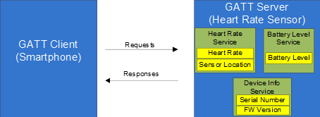
After the Bluetooth® LE connection is established at the link-layer level, the GATT Client (which initially knows nothing about the connected Bluetooth® LE device) initiates a process called “service discovery.” As part of the service discovery, the GATT Client sends multiple requests to the GATT Server to get a list of all the available services, characteristics, and attributes in the GATT Server. When service discovery is complete, the GATT Client has the required information to modify or read the information exposed by the GATT Server using the attribute operations described in the previous section.
Generic Access Profile (GAP)
The GAP layer provides device-specific information such as the device address; device name; and the methods of discovery, connection, and bonding. The Profile defines how a device can be discovered, connected, the list of services available, and how the services can be used. Figure 70 shows an example of a Heart Rate Profile.
The GAP layer operates in one of four roles:
- Peripheral: This is an advertising role that enables the device to connect with a GAP Central. After a connection is established with the central, the device operates as a slave. For example, a heart-rate sensor reporting the measured heart-rate to a remote device operates as a GAP peripheral
- Central: This is the GAP role that scans for advertisements and initiates connections with peripherals. This GAP role operates as the master after establishing connections with peripherals. For example, a smartphone retrieving heart-rate measurement data from a peripheral (heart-rate sensor) operates as a GAP central
- Broadcaster: This is an advertising role that is used to broadcast data. It cannot form Bluetooth® LE connections and engage in data exchange (no request/response operations). This role works similar to a radio station in that it sends data continuously whether or not anyone is listening; it is a one-way data communication. A typical example of a GAP broadcaster is a beacon, which continuously broadcasts information but does not expect any response
- Observer: This is a listening role that scans for advertisements but does not connect to the advertising device. It is the opposite of the broadcaster role. It works similar to a radio receiver that can continuously listen for information but cannot communicate with the information source. A typical example of a GAP Observer is a smartphone app that continuously listens for beacons
Figure 69 shows a generic Bluetooth® LE system with Bluetooth® LE pioneer kit as the peripheral and a smartphone as the central device. The interaction between Bluetooth® LE protocol layers and their roles on the Central and the Peripheral devices are also shown.
Figure 69. Bluetooth® LE system design
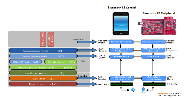
Figure 70 shows an example where a smartphone with a heart-rate app operates as a central and a heart-rate sensor operates as a peripheral. The heart-rate monitoring device implements the Heart-Rate Sensor Profile, while the smartphone receiving the data implements the Heart-Rate Collector profile.
In this example, the Heart-Rate Sensor Profile implements two standard services. The first is a Heart Rate Service that comprises three characteristics (the Heart Rate Measurement Characteristic, the Body Sensor Location Characteristic, and the Heart Rate Control Point Characteristic). The second service is a Device Information Service. At the link layer, the heart-rate measurement device is the slave and the smartphone is the master. See the Bluetooth® developer portal for a detailed description of the Heart Rate Service and Profile.
Figure 70. Bluetooth® LE Heart-rate monitor system
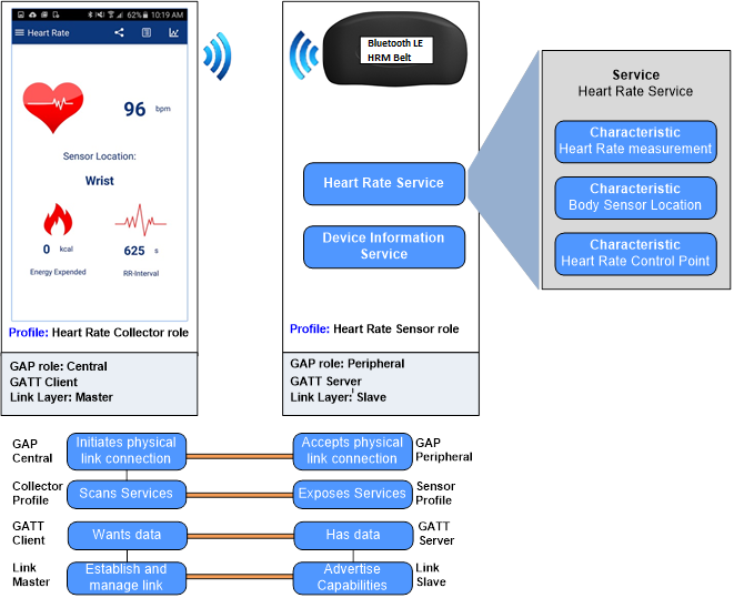
Appendix C. Device features
System wide resources
CPU subsystem: CM4 and CM0
The CPU subsystem in PSoC™ 6-BLE consists of two Cortex® cores: CM4 with a single-precision floating-point unit capable of operating at a maximum frequency of 150 MHz; CM0+ capable of operating at a maximum frequency of 100 MHz. There is a memory protection unit (MPU) available in both the cores. Additionally, there are protection units attached to peripherals called Peripheral Protection Unit (PPUs) and Shared Memory Protection Units (SMPUs) for shared memory regions.
The CM0+ also provides a secure boot function. This allows system integrity to be checked and privileges enforced prior to the execution of the user application.
IPC
Inter-processor communication (IPC) provides the functionality for the two cores to communicate and synchronize their activities. IPC hardware is implemented using register structures in PSoC™ 6-BLE. These register structures are used to synchronize events, and trigger “notify” or “release” events of an IPC channel. PSoC™ 6-BLE supports up to 16 channels, which allows message passing between CPU cores and supports locks for mutual exclusion.
Memory system
The CPU cores have a fixed memory address map that enables shared access to memory and peripherals. Code can be executed from both the flash and RAM on both cores.
The PSoC™ 6-BLE family has up to 1 MB of flash memory and an additional 32 KB of flash that can be used for EEPROM emulation. There is also an additional 32 KB of supervisory flash. In addition, the flash supports Read-While-Write (RWW) operation so that the flash can be written to when the CPU is actively executing instructions. There is also a 128 KB ROM that contains boot and configuration routines. This will ensure Secure Boot operation if authentication of user flash is required for end applications.
PSoC™ 6-BLE has up to 288 KB of SRAM memory, which can be fully retained or retained in increments of user-designated 32 KB blocks.
DMA
The CPU subsystem includes two independent DMA controllers, each capable of running 32 channels. The controllers support independent accesses to the peripherals using the Arm® standard Advanced microcontroller Bus Architecture (AMBA) High-Performance Bus (AHB).
The DMA transfers data to and from memory, peripherals, and registers. These transfers occur independent of the CPU. The DMA channels support the following:
- 8-bit, 16-bit, and 32-bit data widths at both source and destination
- Four priority levels on each channel
- Configurable interrupts on each DMA descriptor
- Descriptor chaining
Clocking system
PSoC™ 6-BLE has the following clock sources:
- Internal main oscillator (IMO): The IMO is the primary source of internal clocking in PSoC™ 6-BLE. The CPU and all high-speed peripherals can operate from the IMO or an external crystal oscillator (ECO). PSoC™ 6-BLE has multiple peripheral clock dividers operating from either the IMO or the ECO, which generate clocks for high-speed peripherals. The IMO can generate an 8 MHz clock with an accuracy of ±1 percent and is available only in Active mode.
- External crystal oscillator (ECO): The PSoC™ 6 MCU device contains an oscillator to drive an external 4 MHz to 33.33 MHz crystal for an accurate clock source
In addition, the external crystal oscillator on the Bluetooth® Low Energy subsystem with a built-in tunable crystal load capacitance is used to generate a highly accurate 32 MHz clock. It is primarily used to clock the Bluetooth® Low Energy subsystem that generates the RF clocks. The high-accuracy ECO clock can also be used as a clock source for the PSoC™ 6-BLE device’s high-frequency clock (CLK_HF) and is designated as the AltHF clock.
- External clock (EXTCLK):The external clock is a megahertz-range clock that can be sourced from a signal on a designated I/O pin. This clock can be used as the source clock for either the PLL or FLL, or it can be used directly by the high-frequency clocks
- Internal low-speed oscillator (ILO):The ILO is a very-low-power 32 kHz oscillator, which primarily generates clocks for low-speed peripherals operating in all power modes
- Precision internal low-speed oscillator (PILO): PILO is an additional source that can provide a more accurate 32.768 kHz clock than ILO. PILO works in Deep Sleep and higher modes
- Watch crystal oscillator (WCO): The 32.768 kHz WCO is used as one of the sources for low frequency clock tree (CLK_LF) along with ILO/PILO. WCO is used to accurately maintain the time interval for Bluetooth® LE advertising and connection events. Similar to ILO, WCO is also available in all modes except the Hibernate and Stop modes
The PSoC™ Bluetooth® LE clock generation system has phase-locked loop (PLL) and frequency-locked loop (FLL) blocks that can be used to generate high-frequency clocks (CLK_HF). These high-frequency clocks in turn drive the CPU core clocks and the peripheral clock dividers.
PSoC™ 6-BLE has five high-frequency root clocks (CLK_HF [0-4]). Each CLK_HF has a destination on the device such as peripherals like serial memory interface.
PSoC™ 6-BLE has clock supervisors on high-frequency clock path 0 (CLK_HF [0]) and WCO to detect if the clock has been stopped and can trigger an interrupt or a system reset or both.
System interrupts
PSoC™ 6-BLE supports interrupts and exceptions on both the CPU cores: CM4 and CM0+. The cores provide their own vector table for handling interrupts/exceptions. PSOC™ 6-BLE can support up to 139 interrupts on CM4 and 32 interrupts on CM0+. Up to 33 interrupts can wake the device from Deep Sleep power mode
Power supply and monitoring
The PSoC™ 6-BLE device family supports an operating voltage of 1.71 V to 3.6 V. It integrates a single-input multiple-output (SIMO) buck converter to power the blocks within the device. The core operating voltage is user selectable between 0.9 V and 1.1 V. The device family supports multiple power supply rails – VDDD, VDDA, VDDIO, and VBACKUP. Additionally, there are power supply rails for Bluetooth® LE radio operation – VDDR. The availability of various supply rails/pins for an application will depend on the device package selected.
The device includes a VBACKUP supply pin to power a small set of peripherals such as RTC and WCO. This rail is independent of all other rails and can exist even when other rails are absent. Because the power supply to these blocks comes from a dedicated VBACKUP pin, these blocks continue to operate even when the device power is disconnected or held in reset. The RTC present in the backup domain provides an option to wake up the device from any power modes.
The PSoC™ 6-BLE family supports power-on reset (POR), brownout detection (BOD), overvoltage protection (OVP), and low-voltage detection (LVD) circuits for power supply monitoring and to implement fail-safe recovery.
For more information on the power supplies in PSoC™ 6-BLE, see the PSoC™ 6 MCU: PSoC™ 63 with BLE architecture technical reference manual.
Power modes
The power modes supported by PSoC™ 6-BLE, in the order of decreasing power consumption, are:
- Active mode: This is the primary mode of operation. In this mode, all peripherals are active and are available
- Low-Power Active mode: This mode is akin to the Active mode with most peripherals operating with limited capability; CPU cores are available. The performance tradeoffs include reduced operating clock frequency, high-frequency clock sources limited in frequency, and lower core operating voltage
- Sleep mode: In this mode, the CPU cores are in Sleep mode, SRAM is in retention, and all peripherals are available. Any interrupt wakes up either of the CPUs and returns the system to Active mode. CM4 and C-M0+ both support their own CPU Sleep modes, and each CPU can be in Sleep independent of the state of the other CPU. The device is said to be in Sleep mode when both the cores are in CPU sleep
- Low-Power Sleep mode: Most peripherals operate with limited capability; CPU cores are not available
- Deep Sleep mode: In Deep Sleep mode, all high-speed clock sources are turned OFF. This in turn makes high-speed peripherals unusable in Deep Sleep. Peripherals that operate on low-frequency clocks only are available
- Hibernate mode: Device and GPIO states are frozen, and the device resets on wakeup
You can use a combination of Sleep, Deep Sleep, and Hibernate modes in a battery-operated Bluetooth® LE system to achieve best-in-class system power with longer battery life. Table 5 shows the dependency between PSoC™ 6-BLE system power modes and BLESS power modes. A check mark in a cell of Table 5 indicates that the BLESS can perform the specified task when the system is in a given power mode. For example, BLESS can be in Deep Sleep mode while the system is in Low-Power Active mode. The retention label indicates that the BLESS operating context is retained when the system switches to Deep Sleep mode.
| BLESS modes | PSoC™ 6-Bluetooth® LE system power modes | |||||
|---|---|---|---|---|---|---|
| Active | Low-Power Active | Sleep | Low-Power Sleep | Deep Sleep | Hibernate | |
| Transmit | ✓ | ✓ | ✓ | ✓ | retention | OFF |
| Receive | ✓ | ✓ | ✓ | ✓ | retention | OFF |
| Idle | ✓ | ✓ | ✓ | ✓ | retention | OFF |
| Deep Sleep | ✓ | ✓ | ✓ | ✓ | retention | OFF |
Secure Boot
Secure booting involves authenticating the application flash images using a key-based security protocol defined by a market/application-specific standard. The secure boot process is implemented in SROM and a separate supervisory flash in the PSoC™ 6-BLE device. The boot code computes a checksum of the boot code and compares it to a value in eFuse. If these values do not match, the boot process fails. The boot code also enforces debug access restrictions as specified in eFuse. Secure boot is an optional feature and needs to be enabled by the end-user.
Programmable digital peripherals
UDB
UDBs are programmable logic blocks that provide functionalities similar to CPLD and FPGA blocks, as Figure 71 shows. UDBs allow you to create a variety of digital functions such as timer, counter, PWM, pseudo random sequence (PRS), CRC, shift register, SPI, UART, I2S, and custom combinational and sequential logic circuits.
Each UDB has two programmable logic devices (PLDs), each with 12 inputs and 8 product terms. PLDs can form registered or combinational sum-of-products logic. Additionally, an 8 bit single-cycle arithmetic logic unit (ALU), known as a “datapath,” is present in each UDB. The datapath helps with the efficient implementation of functions such as timer, counter, PWM, and CRC.
UDBs also provide a switched digital signal interconnect (DSI) fabric that allows signals from peripherals and ports to be routed to and through the UDBs for communication and control.
Figure 71. Universal digital block diagram
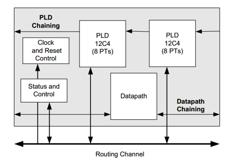
You do not necessarily need to know any hardware description language (HDL) to use UDBs. PSoC™ Creator, development tool for PSoC™ 6-BLE, can generate the required function for you from a schematic. If required, advanced users can implement custom logic on UDBs using Verilog.
PSoC™ 6-BLE has up to 12 UDBs. For more information on UDBs, see the following application notes:
Programmable TCPWM
PSoC™ 6-BLE has 32 programmable TCPWM blocks. Each TCPWM can implement a timer, counter, PWM, or quadrature decoder. TCPWMs provide dead band programmable complementary PWM outputs and selectable start, reload, stop, count, and capture event signals. The PWM mode supports center-aligned, edge, and pseudorandom operations. It also has a kill input to force outputs to a predetermined state.
For more information, refer to the PSoC™ 6-BLE TCPWM component datasheet.
SCB
PSoC™ 6-BLE has up to nine independent run-time programmable SCBs with I2C, SPI, or UART. The SCB supports the following features:
- Standard SPI master and slave functionality with Motorola®, Texas Instruments® Secure Simple Pairing (SSP), and National Semiconductor® Microwire protocols
- Standard UART functionality (up to 1 Mbps baud rate) with smart-card reader, single-wire local interconnect network (LIN) interface, SmartCard (ISO7816), and Infrared Data Association (IrDA) protocols
- Standard I2C master and slave functionality with operating speeds up to 1 Mbps
- EzSPI and EzI2C mode, which allows operation without CPU intervention
- One SCB can be configured to operate in Deep Sleep mode with an external clock. The low-power (Deep Sleep) mode of operation is supported on the SPI and I2C protocols (using an external clock) in slave mode only
For more information, see the PSoC™ 6-BLE SCB Component datasheet.
BLESS
PSoC™ 6-BLE incorporates a Bluetooth® smart subsystem that implements the BLE link layer and physical layer as specified in the Bluetooth® 4.2 specification. The Bluetooth® LE subsystem contains the physical layer (PHY) and link layer engine with an embedded AES-128 security engine. The subsystem supports all Bluetooth® SIG-adopted Bluetooth® LE profiles.
The physical layer consists of a digital PHY and RF transceiver compliant with the Bluetooth® 4.2 specification. The transceiver transmits and receives GFSK packets at 1 Mbps over the 2.4 GHz ISM band. The baseband controller is a composite hardware/firmware implementation that supports both master and slave modes. The key protocol elements such as HCI and link control are implemented in firmware, while time-critical functions such as encryption, CRC, data whitening, and access code correlation are implemented in hardware.
The BLESS is Bluetooth® 4.2 compliant with support for all the features of the Bluetooth® 4.0 specification and some additional features of the Bluetooth® 4.2 specification such as low-duty-cycle advertising, LE ping, L2CAP connection-oriented channels, link layer privacy, link layer data length extension, and LE secure connection. The BLESS block also contains an ECO and WCO that are required for generating an accurate RF frequency and keeping the time between successive connection intervals on the Bluetooth® LE link respectively.
The Bluetooth® LE subsystem supports up to four simultaneous connections. It supports its own four functional power modes: Deep Sleep, Idle, Transmit, and Receive.
Deep Sleep mode
Deep Sleep mode is the lowest power functional mode supported by the BLESS. In this mode, the radio is off. This mode is entered for maximum power saving during an advertising or connection interval after the packet transmission and reception is complete. The ECO can be turned off in this mode for power saving; the WCO, which is the low-frequency clock, is on for maintaining the BLE link layer timing reference logic. The application firmware controls the entry to and exit from this state.
Sleep mode
In Sleep mode, the radio is off. The block maintains all the configurations. The ECO and WCO are turned on, but the clock to the core BLESS logic is turned off. The application firmware controls the entry to and exit from this state.
Idle mode
The Idle mode is the preparation state for the transmit and receive states. In this state, the radio is turned off, but the link layer clock is enabled for the link layer logic so that the CPU starts the protocol state machines.
Transmit mode
Transmit mode is the active functional mode; all the blocks within BLESS are powered on. The link layer clock is enabled to complete the logic within the link layer and RF-PHY. In this mode, RF-PHY gets up to 2 Mbps of serial data from the link layer and transmits the 2.4 GHz GFSK-modulated data to the antenna port. BLESS enters Transmit mode from Idle mode.
Receive mode
This mode enables the BLESS to move into the receive state to perform BLE-specific receiver operations. RF-PHY translates the 1 Mbps data received from the RF analog block and forwards it to the link layer controller after demodulation. A summary of the BLESS power modes and operational sub-blocks is given in Table 6.
| BLESS power mode | ECO | WCO | RF Tx | RF Rx | BLESS Core |
|---|---|---|---|---|---|
| Deep Sleep | Off | On | Off | Off | Off |
| Sleep | On | On | Off | Off | Off |
| Idle | On | On | Off | Off | On |
| Transmit | On | On | On | Off | On |
| Receive | On | On | Off | On | On |
Audio subsystem
PSoC™ 6-BLE has an audio subsystem that consists of an I2S block and two PDM channels. The PDM channels interface to a digital microphone’s bit-stream output. The PDM processing channel provides droop correction and can operate with clock speeds ranging from 384 kHz to 3.072 MHz and produce word lengths of 16 to 24 bits at audio sample rates of up to 48 ksps.
The I2S interface supports both master and slave modes with word clock rates of up to 192 ksps when 8-bit to 32-bit words are transmitted.
Serial Memory Interface
The Serial Memory Interface (SMIF) on PSoC™ 6-BLE is capable of interfacing with different types of memories and up to four memories. SMIF supports Octal-SPI (8 bits/cycle throughput), Dual quad-SPI (8 bits/cycle throughput), quad-SPI (4 bits/cycle throughput), Dual-SPI (2 bits/cycle throughput), and SPI (1 bit/cycle throughput). The block also supports execute-in-place (XIP) mode where the CPU cores can execute code directly from external memory. The SMIF block along with software modules developed in PSoC™ Creator enable you to use a qualified predetermined set of memory devices in your applications.
eFUSE
eFuse is a one-time programmable that is be used to program security-related settings. It can also be used to store your application settings that are programmed once and used later.
Segment LCD
PSoC™ 6-BLE has a segment LCD drive with the following features:
- Supports up to 8 common (COM) and 64 segment (SEG) electrodes
- Programmable GPIOs provide flexible selection of COM and SEG electrodes
- Supports 14-segment and 16-segment alphanumeric display, 7-segment numeric display, dot matrix, and special symbols
- Two drive modes: digital correlation and PWM
- Operates in all system power modes except Hibernate
- Can drive a 3 volt display from 1.8 volt VDD
- Digital contrast control
Programmable analog peripherals
Continuous Time Block Opamps
PSoC™ 6-BLE devices have a pair of Continuous Time Block (CTBm) based opamps that have their inputs and outputs connected to fixed location pins. The opamps support all power modes except Hibernate. However, the opamps operate with reduced gain bandwidth product in Deep Sleep mode. The outputs of these opamps in typical usage can be used as buffers for the SAR inputs.
Low-Power comparator
PSoC™ 6-BLE devices have a pair of low-power comparators that can also operate in Deep Sleep and Hibernate modes. The comparators consume less than 300 nA of current in low-power modes. In a power-sensitive design, when the device goes into low-power mode. you can use the low-power comparator to monitor analog inputs and generate an interrupt that can wake up the system.
For more information, refer to the PSoC™ 6-BLE Low-Power comparator component datasheet.
SAR ADC
PSoC™ 6-BLE has a 12-bit, 1 Msps successive approximation register (SAR) ADC with input channels that support programmable resolution and single-ended or differential input options. The number of GPIOs limits the number of ADC input channels that can be implemented. The SAR ADC does not operate in Deep Sleep and Hibernate modes as it requires a high-speed clock.
The SAR ADC has a hardware sequencer that can perform an automatic scan on as many as eight channels without CPU intervention. The SAR ADC can be connected to a fixed set of pins through an 8-input sequencer. The sequencer cycles through the selected channels autonomously (sequencer scan) and does so with zero switching overhead. It also supports preprocessing operations such as accumulation and averaging of the output data on these eight channels.
You can trigger a scan with a variety of methods, such as firmware, timer, pin, or UDB, giving you additional design flexibility.
To improve the performance in noisy conditions, it is possible to provide an external bypass on a fixed location pin for the internal reference amplifier. For more information on the SAR ADC, see the PSoC™ 6-BLE SAR ADC Component datasheet.
PSoC™ 6-BLE has an on-chip temperature sensor that can be used to measure temperature. The temperature sensor can be connected to the SAR ADC, which digitizes the reading and produces a temperature value by using software Component that includes calibration and linearization.
DAC
PSoC™ 6-BLE has a 12-bit voltage mode continuous time DAC (CTDAC), which has a settling time of 2 µs. The 12-bit DAC provides continuous time output without the need for an external sample and hold (S/H) circuit. The DAC control interface provides an option to control the DAC output through the CPU and DMA. This includes a double-buffered DAC voltage control register, clock input for programmable update rate, interrupt on DAC buffer empty to CPU, and trigger to DMA. The DAC may hence be driven by the DMA controllers to generate user-defined waveforms.
For more information on the DAC, see the PSoC™ 6-BLE DAC Component datasheet.
CAPSENSE
The fourth-generation CAPSENSE™ in the PSoC™ 6-BLE device supports self-capacitance and mutual capacitance-based touch sensing. CAPSENSE™ is supported on all pins.
Capacitive touch sensors use human-body capacitance to detect the presence of a finger on or near a sensor. Capacitive sensors are aesthetically superior, easy to use, and have long lifetimes. The CAPSENSE™ feature in PSoC™ 6-BLE offers best-in-class SNR; best-in-class liquid tolerance; and a wide variety of sensor types such as buttons, sliders, track pads, and proximity sensors.
A software component makes capacitive sensing design very easy; the component supports an automatic hardware-tuning feature called SmartSense and provides a gesture recognition library for trackpads and proximity sensors.
For more information, see the AN85951 - PSoC™ 4 and PSoC™ 6 MCU CAPSENSE™ design guide.
The CAPSENSE™ block has two 7-bit IDACs, which can be used for general purposes if CAPSENSE™ is not using them. A (slow) 10-bit slope ADC may be realized by using one of the IDACs. Refer to the PSoC™ 6-BLE CAPSENSE™ component datasheet for more information on how to use the slope ADC.
Programmable GPIOs
The I/O system provides an interface between the CPU cores, the peripherals, and the external devices. PSoC™ 6-BLE has up to 104 programmable GPIO pins. You can configure the GPIOs for CAPSENSE™, LCD, analog, or digital signals. PSoC™ 6-BLE GPIOs support multiple drive modes, drive strengths, and slew rates.
PSoC™ 6-BLE offers an intelligent routing system that gives multiple choices for connecting an internal signal to a GPIO. This flexible routing simplifies circuit design and board layout.
Additionally, PSoC™ 6-BLE includes up to two Smart I/O ports, which can be used to perform Boolean operations on signals going to and coming from the GPIO pin. Smart I/O ports are also operational in Deep-Sleep mode.
Appendix D. IoT development tools
CY8CKIT-062-BLE PSoC 6-BLE pioneer kit
The PSoC™ 6-BLE pioneer kit shown in Figure 72 is a Bluetooth® LE development kit that supports the
PSoC™ 6-BLE family of devices.
Following are the features of the PSoC™ 6-BLE pioneer kit baseboard:
- Can be powered by a coin-cell battery or through the Type-C USB interface. The Type-C USB interface also supports up to 12 V, 3 A power delivery (PD) consumer and provider profiles
- Enables development of battery-operated low-power Bluetooth® LE designs that work in conjunction with standard, Arduino Uno connector-compliant shields or the onboard PSoC™ 6-BLE device capabilities, such as the CAPSENSE™ user interface and serial memory interface
- Supports third-party programming, debugging, and tracing with the Cortex® Debug/ETM connector
- Includes an additional header that supports interfacing with Pmod™ daughter cards from third-party vendors such as Digilent
- Supports PDM-PCM microphone for voice-over-Bluetooth® LE functionality
- Includes QSPI NOR flash and F-RAM
The kit includes the following:
- A USB-Bluetooth® LE dongle that acts as a Bluetooth® LE link master and works with the CySmart Host Emulation Tool to provide a Bluetooth® LE host emulation platform on non-Bluetooth® LE Windows PCs
- An E-Ink display
The kit consists of a set of BLE example projects and documentation that help you get started on developing your own Bluetooth® LE applications. Visit the CY8CKIT-062-BLE PSoC™ 6-BLE pioneer kit webpage to get the latest updates on the kit and download the kit design, example projects, and documentation files.
Figure 72. CY8CKIT-062-BLE PSoC™ 6-BLE pioneer kit
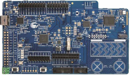
CySmart Host Emulation Tool
The CySmart Host Emulation Tool is a Windows application that emulates a Bluetooth® LE central device using the PSoC™ 6-BLE pioneer kit’s dongle; see Figure 73. It is installed as part of the Bluetooth® LE pioneer kit installation and can be launched by right-clicking the Bluetooth® Low Energy component. It provides a platform for you to test your PSoC™ 6-BLE peripheral implementation over GATT or L2CAP connection-oriented channels by allowing you to discover and configure the Bluetooth® LE services, characteristics, and attributes on your Peripheral.
Operations that you can perform with the CySmart Host Emulation Tool include, but are not limited to:
- Scan Bluetooth® LE peripherals to discover available devices to which you can connect
- Discover available Bluetooth® LE attributes including services and characteristics on the connected Peripheral device
- Perform read and write operations on characteristic values and descriptors
- Receive characteristic notifications and indications from the connected Peripheral device
- Establish a bond with the connected Peripheral device using Bluetooth® LE Security Manager procedures
- Establish a Bluetooth® LE L2CAP connection-oriented session with the Peripheral device and exchange data per the Bluetooth® 4.2 specification
- Perform over-the-air (OTA) firmware upgrade of Bluetooth® LE peripheral devices
Figure 73 and Figure 74 show the user interface of the CySmart Host Emulation Tool. For more information on how to set up and use this tool, see the CySmart user guide from the Help menu.
Figure 73. CySmart Host Emulation Tool Master device tab
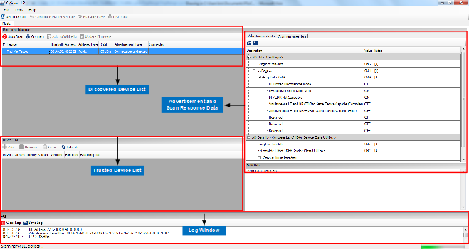
Figure 74. CySmart Host Emulation Tool peripheral device attributes tab
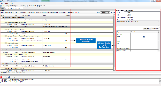
CySmart mobile app
In addition to the PC tool, you can download the CySmart mobile app for iOS or Android from the respective app stores. This app uses the iOS Core Bluetooth® framework and the Android built-in platform framework for Bluetooth® LE respectively. It configures your Bluetooth® LE -enabled smartphone as a Central device that can scan and connect to peripheral devices.
The mobile app supports SIG-adopted Bluetooth® LE standard Profiles through an intuitive GUI and abstracts the underlying Bluetooth® LE service and characteristic details. In addition to the Bluetooth® LE standard profiles, the app demonstrates a custom Profile implementation using LED and CAPSENSE™ demo examples. Figure 75 and Figure 76 show a set of CySmart app screenshots for the Heart Rate Profile user interface. For a description of how to use the app with Bluetooth® LE pioneer kit example projects, see the Bluetooth® LE pioneer kit guide.
Figure 75. CySmart iOS App Heart Rate profile example
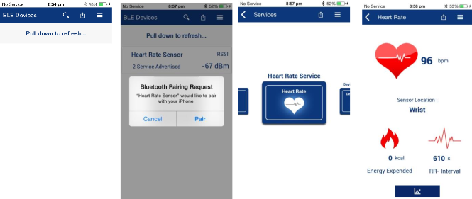
Figure 76. CySmart Android App Heart Rate profile example
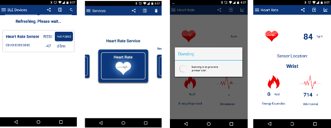
Revision history
| Document version | Date of release | Description of changes |
|---|---|---|
| ** | 2016-12-27 | New Application Note |
| *A | 2017-03-09 | Rewrite of application note Updated UDB template |
| *B | 2017-08-31 | Updated title and figures |
| *C | 2018-04-24 | Partial rewrite of application note Updated template, abstract, and figures |
| *D | 2019-10-11 | Updated title |
| *E | 2022-03-08 | Migrated to Infineon template Replaced BLE with Bluetooth® LE/Bluetooth® Low Energy and PSoC™ 6 BLE to PSoC™ 6-BLE across the document Updated Software version as PSoC™ Creator 4.4 Fixed hyperlinks throughout the document |