About this document
Scope and purpose
AN230938 explains the low-power analog blocks of the PSoC™ 62 MCU CY8C62x4 product line and provides ways to reduce the power consumption in analog sensing applications.
Intended audience
This application note explains how to reduce the power consumption in the analog blocks of the CY8C62x4 product line. For information on reducing power consumption at the chip level with other peripherals, and to know the power modes of the PSoC™ 6 device in general, see AN219528 – PSoC™ 6 MCU Low-Power Modes and Power Reduction Techniques. This application note also provides basic overview of the analog blocks in the CY8C62x4 product line. For detailed information, refer to the Technical Reference Manual (TRM). If you are new to PSoC™ 6, see AN228571 – Getting Started with PSoC™ 6 MCU on ModusToolbox™.
More code examples? We heard you.
To access an ever-growing list of hundreds of PSoC™ code examples, please visit our code examples web page. You can also explore the video training library here.
Introduction
A typical analog front end (AFE) for a measurement system, as Figure 1 shows, involves the use of opamps for filtering and amplification, an analog-to-digital converter (ADC) for digitization, and a CPU for post processing the results. Battery operated systems deploying AFEs pose a challenge in achieving battery life target. In a typical MCU with opamps and ADC, these are significant contributers of power consumption. It becomes critical, specifically in battery-operated systems, to optimize the power levels.
Traditionally, power cycling is used, wherein the MCU is periodically set to low-power state when no measurement is required and is switched to normal power for measurements, resulting in reduced average current. However, in most cases not all peripherals, nor the CPU, need to be active while the ADC is performing the measurements. The CY8C62x4 device achieves significant power savings by allowing only the analog blocks – opamps, ADC, digital-to-analog converter (DAC) and reference to remain ON or power cycle1 in System Deep Sleep mode and collect the measurement results autonomously while rest of the peripherals, including the CPU, are powered off.
The CY8C62x4 product line is unique among the PSoC™ 6 families because it can perform low-power analog sensing. This application note provides an overview of the CY8C62x4 product line and ways to reduce its power consumption. For the evaluation of power consumption, spreadsheet-based calculator can be used from the AN219528 – PSoC™ 6 MCU low-power modes and power reduction techniques.
Programmable analog features
The CY8C62x4 product line has the following rich set of analog features. For an extensive list of peripherals, see the device datasheet.
- Dual opamps
- System Deep Sleep operation with configurable duty-cycling
- Configurable power levels
- Sample and Hold (S/H) circuit (useful with DAC output buffering)
- Two 12-bit, differential input SAR ADCs
- Maximum of 2 Msps sample rate in System LP/ULP Power mode and 100 Ksps in System Deep Sleep mode
- Each ADC allows 16 channels (with 13 unique inputs)
- Scan of all enabled channels without CPU
- Reference sources: 1.2V bandgap, VDDA or external
- Simultaneous sampling
- Deep Sleep operation with duty-cycling
- 64-sample FIFO in each ADC
- Dedicated 16-bit timer for trigger
- Sensor for die temperature measurement
- 12-bit, 500 Ksps DAC
- Reference sources: 1.2 V bandgap (buffered through opamp), external input or VDDA
- Output buffered through opamp
- Ability to hold output in System Deep Sleep state
- 1.2V bandgap reference
- Deep Sleep operation
- Dual low-power comparators
- Ultra Low-power (ULP) mode for operation in System Hibernate mode
- Interrupt generation to wakeup the device
- CAPSENSE™ Capacitive Touch
- Self-capacitance (CSD) and mutual-capacitance sensing (CSX)
- SmartSense auto-tuning
- Dual analog multiplexer buses
- Interconnects GPIOs and analog peripherals
- Ability to split the buses to make multiple connections
- Deep Sleep clock for operating the SAR ADC
Sourced from either 2 MHz Low-Power Oscillator (LPOSC) or Medium Frequency Clock. For the details of each peripheral, see the Technical Reference Manual.
Differences with other PSoC™ 6 devices
Table 1 provides a comparison of CY8C62x4 with other PSoC™ devices.
| Feature | CY8C62x4 | Other PSoC™ 6 devices |
|---|---|---|
|
Number of SAR ADCs |
2 |
1 |
|
Maximum ADC sample rate |
2 Msps in system LP/ULP mode and 100 Ksps in System Deep Sleep mode |
1 Msps/2 Msps2 |
|
SAR ADC in System Deep Sleep mode |
✓ |
× |
|
SAR ADC FIFO |
✓ |
× |
|
Dedicated timer for SAR ADC trigger |
✓3 |
× |
|
Low-power Oscillator (LPOSC) |
✓ |
× |
|
Configurable number of ADC scans per trigger |
✓ |
One scan per trigger or continuous scan |
|
Analog reference in System Deep Sleep mode |
✓ |
✓ |
|
Opamp in System Deep Sleep mode |
Always ON or power cycle |
Always ON |
|
DAC in System Deep Sleep mode4 |
✓ |
✓ |
For more details on low-power operation of analog blocks, see Low-power mode operation of analog resources section.
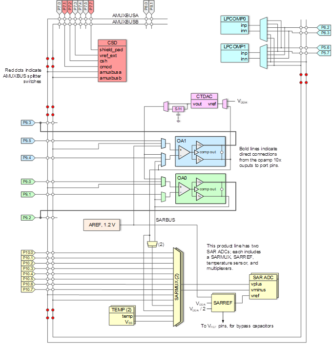
Analog routing
Along with the rich set of analog blocks, CY8C62x4 provides flexible routing to implement circuit configurations that can be dynamically controlled. Figure 2 illustrates the analog routing diagram.
SARMUX: SARMUX is used by the SAR ADC to connect to different sources such as GPIOs, opamp outputs, and temperature sensor. There are two SARMUX blocks in the device, one for each ADC.
SARBUS: SARBUS is used sby the SAR ADC to connect to Opamps via SARMUX. There are two SARBUS blocks: SARBUS0 and SARBUS1.
Analog Multiplexer Bus (AMUXBUS): AMUXBUS is used to interconnect GPIOs from certain ports and to route signals to/from the peripherals. There are two analog mux buses in the device: AMUXBUSA and AMUXBUSB. These buses can be split to create multiple segments which helps to route more than two signals. Note that AMUXBUS connections are not available in Deep Sleep and Hibernate modes. If Deep Sleep or Hibernate operation is required, the Low-power comparator must be connected to the dedicated pins. This restriction also includes routing of any internally-generated signal, which uses the AMUXBUS for the connection.
Dedicated port pins for the peripherals provide slight advantage over other pins in terms of routing resistance and capacitance. See AN218241 – PSoC™ 6 MCU Hardware Design Considerations for the recommended pins.
Low-power mode operation of analog resources
This section describes Deep Sleep operation of analog resources in detail. Table 2 provides the operational capability in different low-power modes.
| Analog resource | System LP/ULP | System deep sleep | System hibernate |
|---|---|---|---|
|
SAR ADCs |
✓ |
✓ |
× |
|
Opamps |
✓ |
✓ |
× |
|
Analog reference (AREF) |
✓ |
✓ |
× |
|
DAC |
✓ |
✓5 |
× |
|
Low-power comparators |
✓ |
✓ |
✓ |
|
CAPSENSE™ |
✓ |
× |
× |
|
AMUXBUS switches |
✓ |
× |
× |
If you are not familiar with the low-power modes of PSoC™ 6, see AN219528 – PSoC™ 6 MCU Low-Power Modes and Power Reduction Techniques.
SAR ADCs
SAR ADCs are supported with resources to operate autonomously in System Deep Sleep mode. These resources include the analog reference generator, LPOSC or medium-frequency clock for running both the SAR ADCs, timer for trigger (common for both ADCs), and a FIFO for storing the data.
The ADCs operate in one of the following two modes:
- Always-ON in LP/ULP mode and powered-OFF in System Deep Sleep mode
- Always-ON in LP/ULP mode and duty-cycling in System Deep Sleep mode
Figure 3 illustrates the operation of an ADC in System Deep Sleep mode and the transition from or to LP/ULP mode.
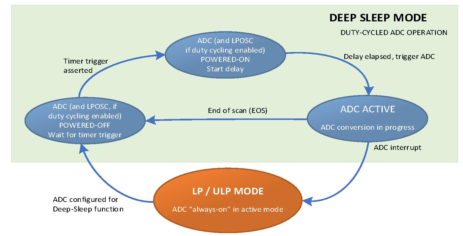
In the LP/ULP mode, the ADC is in an always-on state along with the supporting resources. In the System Deep Sleep mode, the ADC remains powered-off until timer trigger is received. The timer is the only option for an ADC trigger in System Deep Sleep mode. Upon receiving a trigger, a programmable delay (called as power-up delay) is initiated to allow the ADC, the analog reference and LPOSC clock6 to settle before the conversion begins. After this delay, conversion of all enabled channels begins (which corresponds to one scan) and the results are stored in the FIFO. Power for the ADC is then turned OFF and it waits for the next timer trigger.
If both ADCs are used in System Deep Sleep mode, power is not turned OFF until results from both ADCs are moved to their respective FIFOs.
Interrupts are enabled to allow the ADC to wake up the device (see section Interrupts).
Figure 4 illustrates the timing diagram of SAR ADC duty-cycling in System Deep Sleep mode and the resulting average current consumption.
Clock source and limitations
For operating in System Deep Sleep mode, SAR ADC should be clocked from either LPOSC or Medium Frequency Clock. The same clock can be used while operating in System LP/ULP mode. But, using LPOSC or Medium Frequency Clock brings in certain limitation as Table 3 shows.
| Feature | Peripheral clock | LPOSC or medium frequency clock |
|---|---|---|
|
Applicable device operating mode |
System LP/ULP mode |
System LP/ULP mode and System Deep Sleep mode |
|
Maximum clock frequency |
36v MHz |
2 MHz |
|
Trigger source |
Firmware, GPIOs, TCPWMs, Timer or LPCOMP |
Timer |
|
Continuous conversion |
Available |
Not available |
|
Interleaved averaging |
Available |
Not available |
|
Result register |
Available |
Not available (only FIFO) |
|
Collision and overflow interrupt |
Available |
Not available |
|
Injection channel conversion and associated interrupts7 |
Available |
Not available |
Input options
In System Deep Sleep mode, the ADC can receive the inputs from the opamp outputs and from SARMUX port pins. Inputs from other port pins are not available because the AMUXBUS switches do not work in System Deep Sleep mode.
Interrupts
The following interrupts are available to wake up the device from System Deep Sleep mode or when LPOSC/Medium Frequency Clock is used:
- End of Scan (EOS) – Interrupt is generated at the end of conversion of all the enabled channels or after a “Scan Count” number of scans. Scan Count is specified to execute specific number of scans per trigger
- SAR Range Detection – Interrupt is generated when the channel result satisfies the configured condition
- SAR Saturation – Interrupt is generated when the conversion result (before averaging, if enabled) is equal to the minimum or maximum value. This interrupt can individually be enabled for each channel
- FIFO Level – Interrupt is generated when the number of data samples in the FIFO exceeds the configured “Level” value
- FIFO Overflow – Interrupt is generated when new data sample is posted into an already full FIFO
- FIFO Underflow – Interrupt is generated when the CPU or the DMA tries to read an empty FIFO
For a complete list of interrupts, see the ADC chapter in the Technical Reference Manual.
Opamp
Similar to the ADCs, the opamps can also work in System Deep Sleep mode, in the following modes:
- Always-ON in LP/ULP mode and powered-OFF in System Deep Sleep mode
- Always-ON in LP/ULP mode and duty-cycling in System Deep Sleep mode
- Always-ON in LP/ULP mode and System Deep Sleep mode
Note that the ADC does not have a mode (c) available. Opamp mode (c) is useful to avoid wake up times which could be longer with larger external passive components in the opamp feedback path.
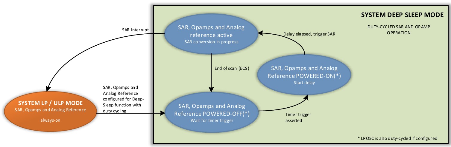
The duty-cycling of opamps is linked to the duty-cycling of the ADCs in System Deep Sleep mode, as Figure 5 shows. Duty-cycling of opamps is possible only when at least one of the ADCs is used in System Deep Sleep mode. The timer trigger wakes up both the opamps and the enabled ADCs. When the conversions are complete, the opamps and ADCs are powered-OFF at the same time. When opamp duty-cycling is not used8 or if the ADCs are configured to operate only in LP/ULP mode, the opamps remain ON continuously throughout the System Deep Sleep time.
Analog reference is used by both the SAR ADCs and the opamps; charge pump is used by Opamps to boost its input range. Their state in System Deep Sleep mode depends on the settings of SAR ADCs and Opamps as Table 4 shows.
| Opamps in system deep sleep mode | Analog reference | Charge pump |
|---|---|---|
|
Powered-OFF |
Always-ON if atleast one of the SAR ADCs is configured for operation in System Deep Sleep mode |
OFF |
|
Duty-cycle |
Duty-cycles |
Duty-cycles |
|
Always-ON |
Always-ON |
OFF |
Power modes
Each opamp has three power settings: high, medium and low; there is additional option to select a 100 nA or a 1 µA current reference from the Analog Reference block which is common for all the opamps in the device. These give a total of six configurable power options for the opamps. Table 5 provides data for the current consumption and gain-bandwidth product while operating the opamp in System Deep Sleep mode.
| Opamp power mode | AREF current9 | Current consumption – typical (µA) | Gain-BW product typical (MHz) |
|---|---|---|---|
|
High |
1 µA |
1300 |
4 |
|
Medium |
1 µA |
460 |
2 |
|
Low |
1 µA |
230 |
0.5 |
|
High |
0.1 µA |
100 |
0.5 |
|
Medium |
0.1 µA |
40 |
0.2 |
|
Low |
0.1 µA |
15 |
0.1 |
Higher the power setting, higher the gain-bandwidth product and higher the current consumption for a given AREF current. Power setting also affects other opamp parameters. Refer the device datasheet for details.
DAC
DAC, in System Deep Sleep mode, can hold its last configured value. It is not possible to change this value during System Deep Sleep mode. This voltage is buffered using CTBm opamp and driven to a pin. This is useful in applications, where voltage is continuously required for biasing.
There is another useful feature of duty-cycling the DAC which works in conjunction with S/H circuit of CTBm. In this method, firmware connects DAC output to Opamp input in order to sample the DAC output and then DAC is disconnected and powered down. Opamp input is held at a certain potential which is periodically refreshed using firmware. Figure 6 shows a simplified diagram of S/H between DAC and opamp. For the detailed configuration, refer the Technical Reference Manual.
Analog reference (AREF)
The AREF block generates voltage and current references required for SAR ADCs, Opamps, DAC and CAPSENSE™. This block can operate in both System LP/ULP and System Deep Sleep modes. In the System Deep Sleep mode, AREF block can be configured in different modes as Table 6 shows.
| AREF setting | Details |
|---|---|
|
Disabled |
OFF |
|
Fast wakeup |
This mode is useful for fast startup from disabled state to active state while transitioning from System Deep Sleep mode to System LP/ULP mode. Reference voltage and current are not available in System Deep Sleep mode. |
|
Opamp reference current enabled |
In this mode, AREF provides reference current to the CTBm Opamps. No voltage reference is available. |
|
All references enabled |
In this mode, voltage and current references are available. As explained in the Opamp section, AREF is required for opamp to operate in Deep Sleep mode, therefore AREF also needs to duty-cycle if the opamp is configured to duty-cycle in System Deep Sleep mode. |
AREF current, available to the CTBm opamps, can be configured to either 100 nA or 1 μA which affects the power consumption (see Table 5).
Low-power comparator (LPCOMP)
LPCOMP is the only analog block capable of operating even in Hibernate mode. There are two LPCOMPs in the device. It provides an option to generate interrupt so as to wake up the device. The block provides three programmable power levels: normal, low, and ultra-low. The response time of the block increases with the decrease in the power level as Table 7 shows.
| LPCOMP power mode | Current consumption – maximum (µA) | Response time – maximum (µs) |
|---|---|---|
|
Normal |
150 |
0.1 |
|
Low |
10 |
1 |
|
Ultra-Low |
0.85 |
20 |
Power mode selection also impacts other parameters of the block. Refer the device datasheet for the specifications.
Power optimization techniques
This section provides different ways to reduce the power consumption while using analog blocks of the device.
Power modes of the block
Opamps and LPCOMPs provide configurable power options. Depending on the application requirement, block power can be optimized. Note that lower power levels come with a penalty on the performance. Refer the Opamp section and Low-power comparator (LPCOMP) section for details.
Duty-cycling the blocks
Many applications do not require continuous scanning of analog inputs and the CPU in its operation in the field. In such cases, duty-cycling of analog sources in System Deep Sleep mode yields significant power savings. Following sections describe three scenarios with the use of duty-cycling for SAR ADC and Opamp. Bench current measurement is done using the CY8CKIT-062S4 PSoC™ 62S4 Pioneer Kit.
Example: SAR ADC
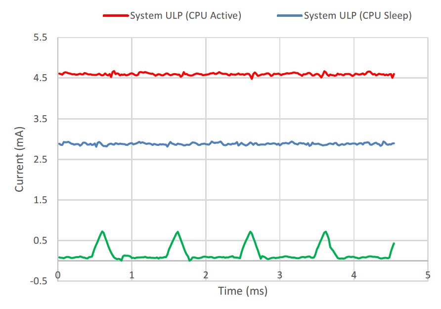
Consider an application which uses one SAR ADC. Table 8 and Figure 7 provides power consumption results for the device for two cases – when the SAR ADC is operated in System ULP mode and when duty-cycling is used in System Deep Sleep mode.
| Device power mode | Average device current (mA) | Conditions |
|---|---|---|
|
System ULP mode (CPU Active) |
4.59 |
CPU is in active state executing loop instruction. SAR ADC is always powered-ON, sampling periodically at 1 kHz with the scan time of 1 ms. |
|
System ULP mode (CPU Sleep) |
2.87 |
CPU is set to sleep, SAR ADC is always powered-ON, sampling periodically at 1 kHz with the scan time of 1 ms. |
|
System Deep Sleep mode |
0.17 |
SAR ADC power is duty-cycled and it samples periodically at 1 kHz with the scan time of 1 ms. Interrupt is disabled to keep the device in System Deep Sleep. |
The current measurement in Figure 7 setup uses the following key settings:
- Core Regulator: ULP, Normal Current LDO
- PLL Frequency: 50 MHz, FLL: Disabled
- CM4 Frequency: 50 MHz
- VDDA: 3.3 V
SAR is configured with following settings:
- SAR Clock: Duty-cycled LPOSC 2 MHz
- Vref: VDDA
- Acquisition time: 1 µs
- Number of channels: 1
- Timer frequency/period: 1 kHz/1 ms
- Timer clock input: ILO
- Averaging: Enabled- 16 samples
- Power-up delay: 20 µs
- Calculated conversion time (scan time): 136 µs
Example: SAR ADC + opamp
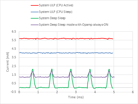
For the application with opamp buffer output connected to SAR ADC, Table 9 and Figure 8 provides the bench current measurement results. Three uses cases demonstrated: both the SAR ADC and opamp operated in System ULP mode without duty-cycling, with duty-cycled SAR ADC and always-ON Opamp in System Deep Sleep mode and with duty-cycled SAR ADC and Opamp in System Deep Sleep mode.
| Device power mode | Average device current (mA) | Conditions |
|---|---|---|
|
System ULP mode (CPU is active) |
5.7 |
CPU is in active state executing loop instruction. SAR ADC and opamp are always powered-ON, SAR sampling the opamp output periodically at 1 kHz with the scan time of 1 ms. In this case, opamp charge pump is enabled with peripheral clock. |
|
System ULP mode (CPU in sleep) |
4.03 |
CPU is set to sleep, SAR ADC and opamp are always powered-ON, SAR samples the opamp output periodically at 1 kHz with the scan time of 1 ms. In this case, the opamp charge pump is enabled with peripheral clock. |
|
System Deep Sleep mode with Opamp always-ON |
1.32 |
SAR ADC power is duty-cycled and opamp is always ON. SAR ADC samples periodically at 1 kHz with the scan time of 1 ms. Interrupt is disabled; hence CPU never gets woken up. In this case, the opamp charge pump is disabled, resulting in reduced input range. |
|
System Deep Sleep mode with Opamp duty-cycled |
0.32 |
SAR ADC and opamp power are duty-cycled. SAR ADC samples periodically at 1 kHz with the scan time of 1 ms. Interrupt is disabled to keep the device in System Deep Sleep mode. In this case, the opamp charge pump is enabled with LPOSC clock. |
The current measurement in Figure 8 setup uses the following key settings:
- Core Regulator: ULP, Normal Current LDO
- PLL Frequency: 50 MHz, FLL: Disabled
- CM4 Frequency: 50 MHz
- VDDA: 3.3 V
SAR is configured with following settings:
- SAR Clock: Duty-cycled LPOSC 2 MHz
- Vref: VDDA
- Acquisition time: 1 µs
- Number of channels: 1
- Timer frequency/period: 1 kHz/1 ms
- Timer clock input: ILO
- Averaging: Enabled- 16 samples
- Power-up delay: 20 µs10
- Calculated conversion time (scan time): 136 µs
Opamp is configured with following settings:
- Follower configuration
- Power mode: High
- AREF current: 1 µA
- Pump clock: 24 MHz System Resources Pump Clock or 2 MHz LPOSC clock
The Low Power Analog Front- End using OpAmp and SAR ADC code example available on GitHub can be used as reference to get started with configuring and programming for low power designs.
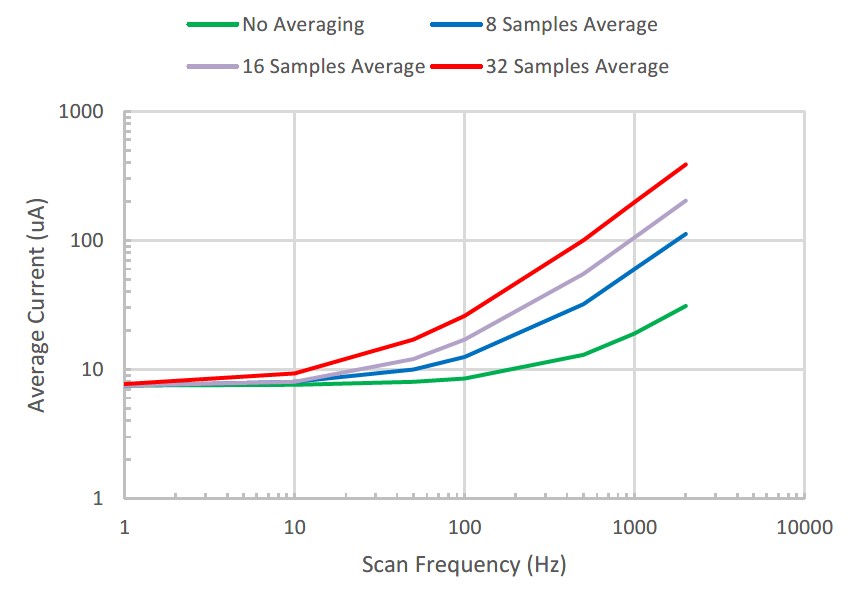
SAR ADC scan frequency
One scan of SAR ADC involves sampling and conversion of all the enabled channels. When duty-cycling is used, power savings depend on the interval between the two scans triggered by the Timer. Longer the interval, that is lower the scan frequency, lower the power consumption. For applications where the signal to be measured vary slowly, the scan interval should be set longer.
Based on the test settings provided in Example: SAR ADC section (except for the timer clock input; here, WCO is used instead of ILO for better accuracy), Figure 9 shows current numbers with the bench testing with CY8CKIT-062S4 PSoC™ 62S4 Pioneer Kit for different scan frequencies and average sample count while operating in System Deep Sleep mode.
SAR ADC acquisition time
Acquisition time of SAR ADC channels should be set to minimum possible value to reduce the operating time of SAR ADC and power consumption. Acquisition time is selected from one of the four programmable 10-bit fields. If the SAR ADC clock is set to peripheral clock of 36 MHz (maximum frequency), the acquisition time can be set from 83 ns (three clocks) to 28 µs. With 2 MHz LPOSC or Medium Frequency Clock, the acquisition time can be set from 0.5 µs (1 clock) to 512 µs. Selection of the acquisition time depends on the source resistance, input resistance, and input capacitance of SAR ADC.
Figure 10 shows the equivalent diagram of the SAR ADC input. When the acquisition begins with the closing of SWACQ, the CHOLD charges towards the input signal value. For 12-bit resolution, it takes 9RC time to charge within ½ LSB of the final value. Therefore, the minimum acquisition time is as shown below.
TACQ ≥ 9 × R × CHOLD
where,
R = RSRC + RSW1 + RSW2
RSRC = Source resistance
RSW1 = SAR sampling switch resistance
RSW2 = Routing resistance
C = CHOLD is the SAR input capacitance and it is typically 5pF
If the input is taken from SARMUX port pins, RSW1 + RSW2 is typically 1 kΩ. If routing involves SARBUS or AMUX bus, additional resistance should be included which results in increased acquisition time requirement. It is therefore recommended to use SARMUX port pins for SAR ADC inputs.
SAR ADC reference buffer
Each SAR ADC includes a reference buffer to drive its reference. The input options to the reference buffer are the 1.2 V from Analog Reference block and VDDA/2. The other options (VDDA and external reference from the GPIO) are connected directly to the reference terminal of SAR ADC and the reference buffer is disabled. Thus, power can be saved if VDDA or external reference is used. Refer the device datasheet for the current consumption with internal and external reference specifications.
Reference buffer power can be adjusted based on the SAR ADC clock frequency. ModusToolbox™ software automatically configures the buffer power based on the selected clock frequency. If SAR ADC is configured manually, then buffer power should be configured to 100% when operating above 18 MHz, 60% when operating at 3.6 MHz to 18 MHz, and 30% when operating below 3.6 MHz. Refer the Technical Reference Manual for more details.
The reference buffer output can be routed to pin for filtering using a bypass capacitor11. Start up time of the SAR ADC block varies with the capacitor used for the internal reference voltage filtering as Table 10 shows.
| Reference and Bypass Capacitor | Maximum Start Up Time (µs) |
|---|---|
|
Internal reference without bypass capacitor, external or VDDA reference |
10 |
|
Internal reference with 100 nF |
210 |
LPOSC or medium frequency clock
SAR ADC is clocked from one of the two options for operating in System Deep Sleep mode. Medium Frequency Clock is derived from System Deep Sleep operable Internal Main Oscillator (IMO) which consumes slightly more current than the LPOSC with the identical accuracy. LPOSC can be duty-cycled as explained in LPOSC duty-cycling section below. Therefore, use the LPOSC for additional power savings.
LPOSC duty-cycling
LPOSC provides an option to duty-cycle along with SAR ADC power, thus, providing power savings while SAR is powered-down in System Deep Sleep mode. If SAR ADC is configured to use Medium Frequency Clock, turn OFF the LPOSC to save power. When duty-cycling is enabled for LPOSC, ensure the Timer (which is the only trigger source in System Deep Sleep mode) is clocked using ILO or WCO.
Power-up delay
As described in SAR ADCs section, power-up delay allows the SAR ADC (mainly, the reference buffer), Analog Reference, LPOSC and Opamp (if used with duty-cycling) to settle before sampling and conversion process begins. Power-up delay is an 8-bit configuration value, clocked from either LPOSC or Medium Frequency Clock selected for the SAR ADC; i.e., Power-up delay can range from 0 to 127.5 µs.
The minimum value of power-up delay required is 20 µs. If your design includes external elements that require more settling time, increase the delay until there is no transient in the output. If the maximum delay is reached and output still has transient, modify your design to reduce the settling time required or throw away the initial few samples.
FIFO chain
Each SAR ADC in the device is equipped with its own FIFO of 64 samples depth to collect the measurement results in System Deep Sleep mode. FIFO chaining is possible wherein, FIFO associated with the second SAR ADC (SAR ADC 1) is chained to the FIFO of the first SAR ADC (SAR ADC 0), thereby, doubling the depth of the resulting FIFO. Note that this combined FIFO will load results only from SAR ADC 0. It helps to load larger number of results, while being in System Deep Sleep mode; thus, saving the power. Use FIFO chaining whenever faster sampling is used or when CPU processing is performed on large samples at a slower rate.
DMA
When the device wakes up, there are two options to read the FIFO data: using CPU or DMA. Using DMA saves the power and is useful when larger samples are required to be accumulated which cannot fit even in the chained FIFO. In this case, DMA can be used to move the FIFO data into memory when the CPU is in Sleep mode. When the required number of samples are accumulated, CPU can then be woken up for processing.
Summary
This application note provides an overview of the PSoC™ 62 MCU CY8C62x4, its low-power features and suggestions for implementing power-efficient applications.
References
Application Notes
Code Examples
Revision history
| Document version | Date of release | Description of changes |
|---|---|---|
|
** |
2021-07-02 |
Initial release. |
| *A | 2022-07-21 | Template update. |
| *B | 2023-12-07 | Completing Sunset review. Updated reference links. |